General-purpose timers (TIM9 to TIM14) RM0008
437/1128 DocID13902 Rev 15
16.3.12 Timer synchronization (TIM9/12)
The TIM timers are linked together internally for timer synchronization or chaining. Refer to
Section 15.3.15: Timer synchronization on page 391 for details.
16.3.13 Debug mode
When the microcontroller enters debug mode (Cortex
®
-M3 core halted), the TIMx counter
either continues to work normally or stops, depending on DBG_TIMx_STOP configuration
bit in DBG module. For more details, refer to Section 31.16.2: Debug support for timers,
watchdog, bxCAN and I2C.
16.4 TIM9 and TIM12 registers
Refer to Section 2.1 on page 47 for a list of abbreviations used in register descriptions.
The peripheral registers have to be written by half-words (16 bits) or words (32 bits). Read
accesses can be done by bytes (8 bits), half-words (16 bits) or words (32 bits).
16.4.1 TIM9/12 control register 1 (TIMx_CR1)
Address offset: 0x00
Reset value: 0x0000
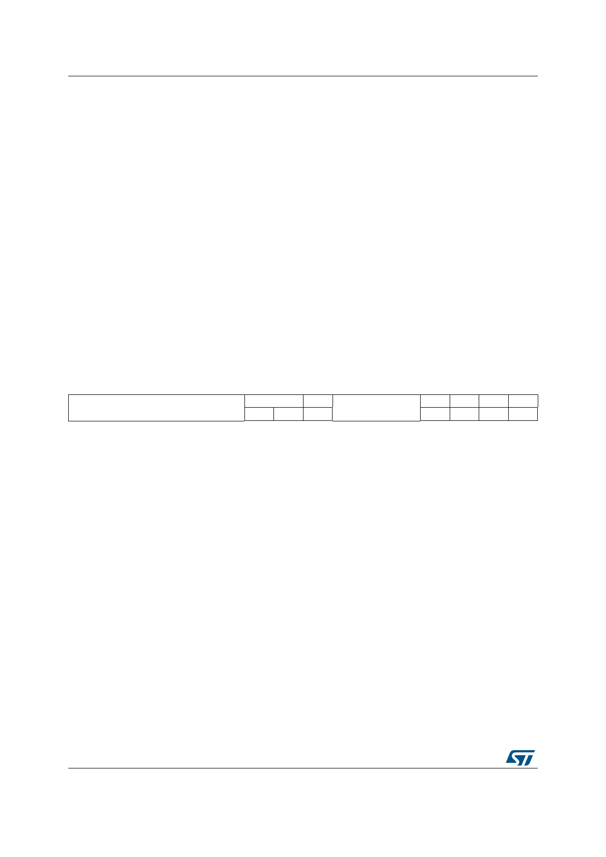
1514131211109876543210
Reserved
CKD[1:0] ARPE
Reserved
OPM URS UDIS CEN
rw rw rw rw rw rw rw
Bits 15:10 Reserved, must be kept at reset value.
Bits 9:8 CKD: Clock division
This bit-field indicates the division ratio between the timer clock (CK_INT) frequency and
sampling clock used by the digital filters (TIx),
00: t
DTS
= t
CK_INT
01: t
DTS
= 2 × t
CK_INT
10: t
DTS
= 4 × t
CK_INT
11: Reserved
Bit 7 ARPE: Auto-reload preload enable
0: TIMx_ARR register is not buffered.
1: TIMx_ARR register is buffered.
Bits 6:4 Reserved, must be kept at reset value.
Bit 3 OPM: One-pulse mode
0: Counter is not stopped on the update event
1: Counter stops counting on the next update event (clearing the CEN bit).
 Loading...


