General-purpose timers (TIM2 to TIM5) RM0008
411/1128 DocID13902 Rev 15
Note: The state of the external IO pins connected to the standard OCx channels depends on the
OCx channel state and the GPIO and AFIO registers.
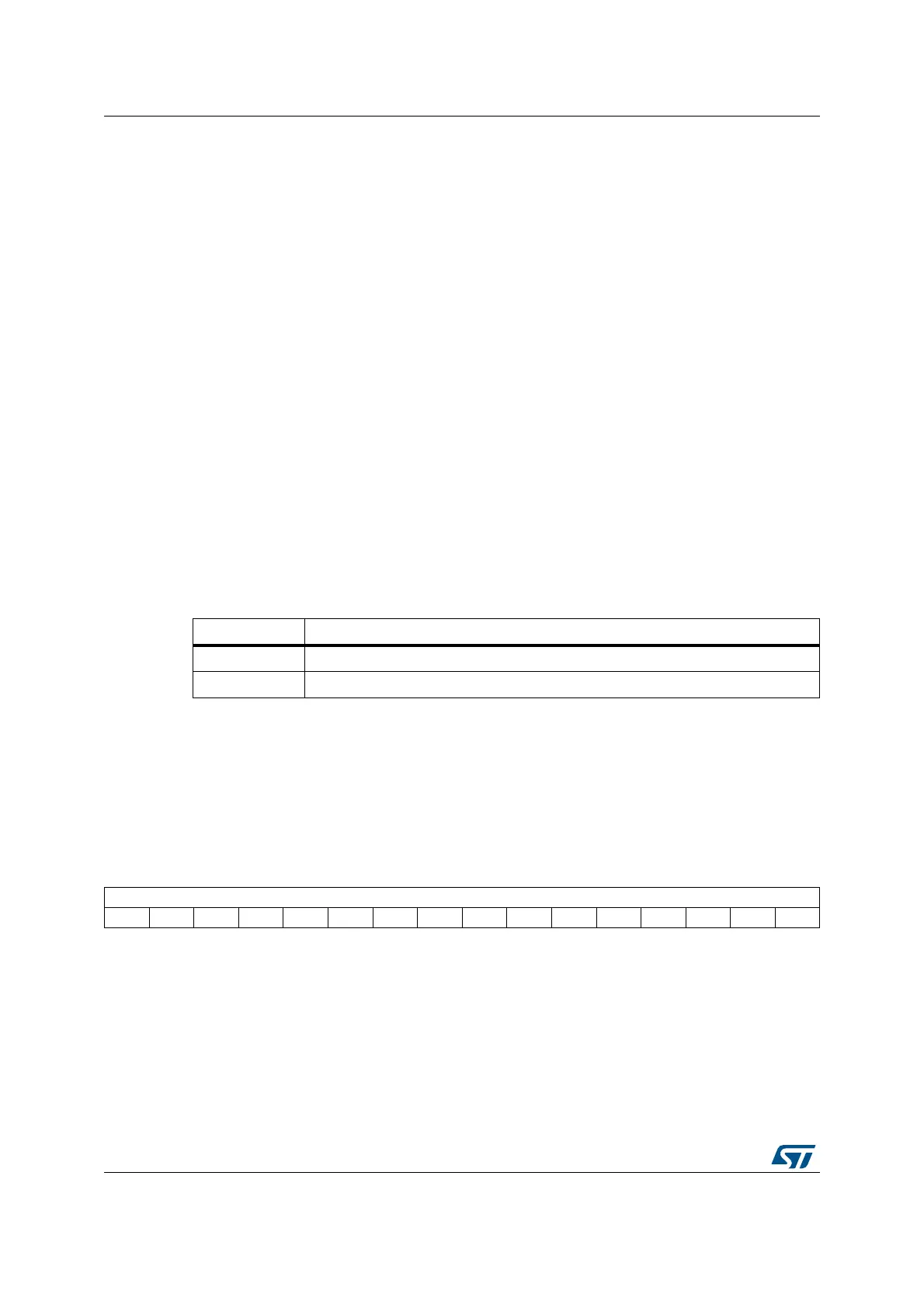
15.4.10 TIMx counter (TIMx_CNT)
Address offset: 0x24
Reset value: 0x0000
Bit 4 CC2E: Capture/Compare 2 output enable
refer to CC1E description
Bits 3:2 Reserved, must be kept at reset value.
Bit 1 CC1P: Capture/Compare 1 output polarity
CC1 channel configured as output:
0: OC1 active high.
1: OC1 active low.
CC1 channel configured as input:
This bit selects whether IC1 or IC1 is used for trigger or capture operations.
0: non-inverted: capture is done on a rising edge of IC1. When used as external trigger, IC1
is non-inverted.
1: inverted: capture is done on a falling edge of IC1. When used as external trigger, IC1 is
inverted.
Bit 0 CC1E: Capture/Compare 1 output enable
CC1 channel configured as output:
0: Off - OC1 is not active.
1: On - OC1 signal is output on the corresponding output pin.
CC1 channel configured as input:
This bit determines if a capture of the counter value can actually be done into the input
capture/compare register 1 (TIMx_CCR1) or not.
0: Capture disabled.
1: Capture enabled.
Table 87. Output control bit for standard OCx channels
CCxE bit OCx output state
0 Output Disabled (OCx=0, OCx_EN=0)
1 OCx=OCxREF + Polarity, OCx_EN=1
1514131211109876543210
CNT[15:0]
rw rw rw rw rw rw rw rw rw rw rw rw rw rw rw rw
Bits 15:0 CNT[15:0]: Counter value
 Loading...


