Backup registers (BKP) RM0008
83/1128 DocID13902 Rev 15
6.4 BKP registers
Refer to Section 2.1 on page 47 for a list of abbreviations used in register descriptions.
The peripheral registers can be accessed by half-words (16-bit) or words (32-bit).
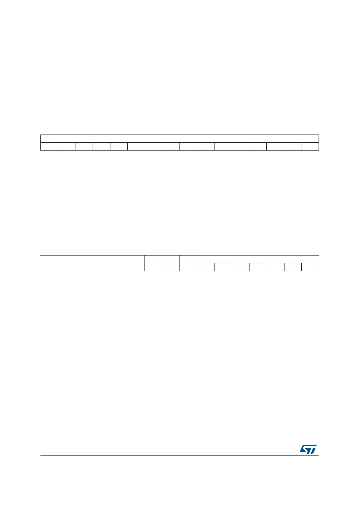
6.4.1 Backup data register x (BKP_DRx) (x = 1 ..42)
Address offset: 0x04 to 0x28, 0x40 to 0xBC
Reset value: 0x0000 0000
6.4.2 RTC clock calibration register (BKP_RTCCR)
Address offset: 0x2C
Reset value: 0x0000 0000
15 14131211109876543210
D[15:0]
rw rw rw rw rw rw rw rw rw rw rw rw rw rw rw rw
Bits 15:0 D[15:0] Backup data
These bits can be written with user data.
Note: The BKP_DRx registers are not reset by a System reset or Power reset or when the
device wakes up from Standby mode.
They are reset by a Backup Domain reset or by a TAMPER pin event (if the TAMPER
pin function is activated).
1514131211109876543210
Reserved
ASOS ASOE CCO CAL[6:0]
rw rw rw rw rw rw rw rw rw rw
Bits 15:10 Reserved, must be kept at reset value.
Bit 9 ASOS: Alarm or second output selection
When the ASOE bit is set, the ASOS bit can be used to select whether the signal output on
the TAMPER pin is the RTC Second pulse signal or the Alarm pulse signal:
0: RTC Alarm pulse output selected
1: RTC Second pulse output selected
Note: This bit is reset only by a Backup domain reset.
 Loading...


