DocID13902 Rev 15 376/1128
RM0008 General-purpose timers (TIM2 to TIM5)
417
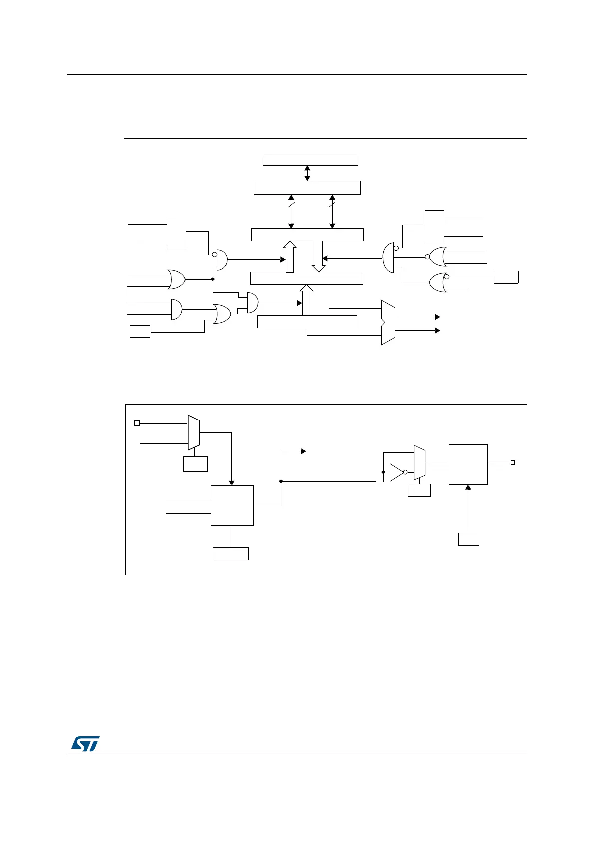
The output stage generates an intermediate waveform which is then used for reference:
OCxRef (active high). The polarity acts at the end of the chain.
Figure 126. Capture/compare channel 1 main circuit
Figure 127. Output stage of capture/compare channel (channel 1)
The capture/compare block is made of one preload register and one shadow register. Write
and read always access the preload register.
In capture mode, captures are actually done in the shadow register, which is copied into the
preload register.
In compare mode, the content of the preload register is copied into the shadow register
which is compared to the counter.
CC1E
Capture/Compare Shadow Register
comparator
Capture/Compare Preload Register
Counter
IC1PS
CC1S[0]
CC1S[1]
capture
input
mode
S
R
read CCR1H
read CCR1L
read_in_progress
capture_transfer
CC1S[0]
CC1S[1]
S
R
write CCR1H
write CCR1L
write_in_progress
output
mode
UEV
OC1PE
(from time
compare_transfer
APB Bus
8
8
high
low
(if 16-bit)
MCU-peripheral interface
TIMx_CCMR1
OC1PE
base unit)
CNT>CCR1
CNT=CCR1
TIMx_EGR
CC1G
KƵƚƉƵƚŵŽĚĞ
EdхZϭ
EdсZϭ
ĐŽŶƚƌŽůůĞƌ
d/DdžͺDZϭ
KϭDϮϬ
ŽĐϭƌĞĨ
Ϭ
ϭ
ϭW
d/DdžͺZ
KƵƚƉƵƚ
ŶĂďůĞ
ŝƌĐƵŝƚ
Kϭ
ϭ
d/DdžͺZ
dŽƚŚĞŵĂƐƚĞƌŵŽĚĞ
ĐŽŶƚƌŽůůĞƌ
dZ&
Ϭ
ϭ
KZ&ͺ>Z
KZ&ͺ>Zͺ/Ed
K^
d/Ddžͺ^DZ
Ăŝϭϳϭϴϳ
 Loading...


