DocID13902 Rev 15 156/1128
RM0008 Connectivity line devices: reset and clock control (RCC)
158
8.3.13 RCC register map
The following table gives the RCC register map and the reset values.
Bits 3:0 PREDIV1[3:0]: PREDIV1 division factor
Set and cleared by software to select PREDIV1 division factor. These bits can be written only
when PLL is disabled.
Note: Bit(0) is the same as bit(17) in the RCC_CFGR register, so modifying bit(17) in the
RCC_CFGR register changes Bit(0) accordingly.
0000: PREDIV1 input clock not divided
0001: PREDIV1 input clock divided by 2
0010: PREDIV1 input clock divided by 3
0011: PREDIV1 input clock divided by 4
0100: PREDIV1 input clock divided by 5
0101: PREDIV1 input clock divided by 6
0110: PREDIV1 input clock divided by 7
0111: PREDIV1 input clock divided by 8
1000: PREDIV1 input clock divided by 9
1001: PREDIV1 input clock divided by 10
1010: PREDIV1 input clock divided by 11
1011: PREDIV1 input clock divided by 12
1100: PREDIV1 input clock divided by 13
1101: PREDIV1 input clock divided by 14
1110: PREDIV1 input clock divided by 15
1111: PREDIV1 input clock divided by 16
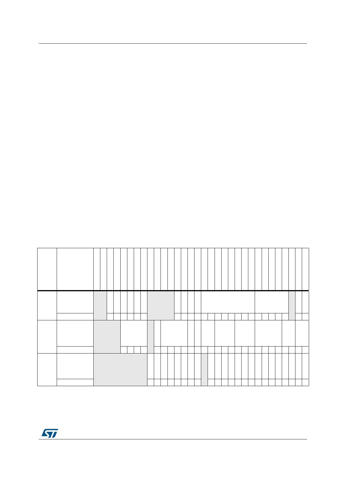
Table 19. RCC register map and reset values
Offset Register
31
30
29
28
27
26
25
24
23
22
21
20
19
18
17
16
15
14
13
12
11
10
9
8
7
6
5
4
3
2
1
0
0x000
RCC_CR
Rese
rved
PLL3 RDY
PLL3 ON
PLL2 RDY
PLL2 ON
PLL RDY
PLLON
Reserved
CSSON
HSEBYP
HSERDY
HSEON
HSICAL[7:0] HSITRIM[4:0]
Reserved
HSIRDY
HSION
Reset value 000000 0000xxxxxxxx10000 11
0x004
RCC_CFGR
Reserved
MCO [3:0]
Reserved
OTGFSPRE
PLLMUL
[3:0]
PLLXTPRE
PLLSRC
ADC
PRE
[1:0]
PPRE2
[2:0]
PPRE1
[2:0]
HPRE[3:0]
SWS
[1:0]
SW
[1:0]
Reset value
0000 00000000000000000000000
0x008
RCC_CIR
Reserved
CSSC
PLL3RDYC
PLL2RDYC
PLLRDYC
HSERDYC
HSIRDYC
LSERDYC
LSIRDYC
Reserved
PLL3RDYIE
PLL2RDYIE
PLLRDYIE
HSERDYIE
HSIRDYIE
LSERDYIE
LSIRDYIE
CSSF
PLL3RDYF
PLL2RDYF
PLLRDYF
HSERDYF
HSIRDYF
LSERDYF
LSIRDYF
Reset value 00000000 000000000000000
 Loading...


