DocID13902 Rev 15 252/1128
RM0008 Analog-to-digital converter (ADC)
252
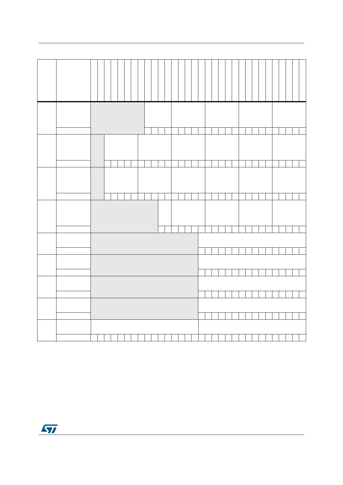
Refer to Table 1 on page 24 for the register boundary addresses.
0x2C
ADC_SQR1
Reserved
L[3:0]
SQ16[4:0] 16th
conversion in
regular
sequence bits
SQ15[4:0] 15th
conversion in
regular
sequence bits
SQ14[4:0] 14th
conversion in
regular
sequence bits
SQ13[4:0] 13th
conversion in
regular
sequence bits
Reset value 000000000000000000000000
0x30
ADC_SQR2
Reserved
SQ12[4:0] 12th
conversion in
regular
sequence bits
SQ11[4:0] 11th
conversion in
regular
sequence bits
SQ10[4:0] 10th
conversion in
regular
sequence bits
SQ9[4:0] 9th
conversion in
regular
sequence bits
SQ8[4:0] 8th
conversion in
regular
sequence bits
SQ7[4:0] 7th
conversion in
regular
sequence bits
Reset value 000000000000000000000000000000
0x34
ADC_SQR3
Reserved
SQ6[4:0] 6th
conversion in
regular
sequence bits
SQ5[4:0] 5th
conversion in
regular
sequence bits
SQ4[4:0] 4th
conversion in
regular
sequence bits
SQ3[4:0] 3rd
conversion in
regular
sequence bits
SQ2[4:0] 2nd
conversion in
regular
sequence bits
SQ1[4:0] 1st
conversion in
regular
sequence bits
Reset value 000000000000000000000000000000
0x38
ADC_JSQR
Reserved
JL[1:
0]
JSQ4[4:0] 4th
conversion in
injected
sequence bits
JSQ3[4:0] 3rd
conversion in
injected
sequence bits
JSQ2[4:0] 2nd
conversion in
injected
sequence bits
JSQ1[4:0] 1st
conversion in
injected
sequence bits
Reset value 0000000000000000000000
0x3C
ADC_JDR1
Reserved
JDATA[15:0]
Reset value 0000000000000000
0x40
ADC_JDR2
Reserved
JDATA[15:0]
Reset value 0000000000000000
0x44
ADC_JDR3
Reserved
JDATA[15:0]
Reset value 0000000000000000
0x48
ADC_JDR4
Reserved
JDATA[15:0]
Reset value 0000000000000000
0x4C
ADC_DR ADC2DATA[15:0] Regular DATA[15:0]
Reset value 00000000000000000000000000000000
Table 72. ADC register map and reset values (continued)
Offset Register
31
30
29
28
27
26
25
24
23
22
21
20
19
18
17
16
15
14
13
12
11
10
9
8
7
6
5
4
3
2
1
0
 Loading...


