EasyManua.ls Logo

Texas Instruments TMS320C6455 User Manual

Texas Instruments TMS320C6455
257 pages
To Next Page IconTo Next Page
To Previous Page IconTo Previous Page
Page #22 background image
ACE4
(A)
AECLKOUT
AED[63:0]
ACE3
(A)
ACE2
(A)
AEA[19:0]
AARDY
Data
Memory Map
Space Select
Address
Byte Enables
64
20
External
Memory I/F
Control
EMIFA (64-bit Data Bus)
AECLKIN
AHOLD
AHOLDA
ABUSREQ
Bus
Arbitration
ABE3
ABE2
ABE1
ABE0
ASWE/AAWE
DDR2CLKOUT
DED[31:0]
DCE0
DEA[13:0]
Data
Memory Map
Space Select
Address
Byte Enables
32
14
External
Memory I/F
Control
DDR2 Memoty Controller (32-bit Data Bus)
DSDCAS
DSDCKE
DDR2CLKOUT
DSDDQS[3:0]
DSDRAS
DSDWE
DSDDQS[3:0]
ABE7
ABE6
ABE5
ABE4
ACE5
(A)
Bank Address
ABA[1:0]
AR/W
AAOE/ASOE
ASADS/ASRE
Bank Address
DBA[2:0]
DEODT[1:0]
DSDDQGATE[0]
DSDDQM3
DSDDQM2
DSDDQM1
DSDDQM0
DSDDQGATE[1]
DSDDQGATE[2]
DSDDQGATE[3]
TMS320C6455
SPRS276M MAY 2005REVISED MARCH 2012
www.ti.com
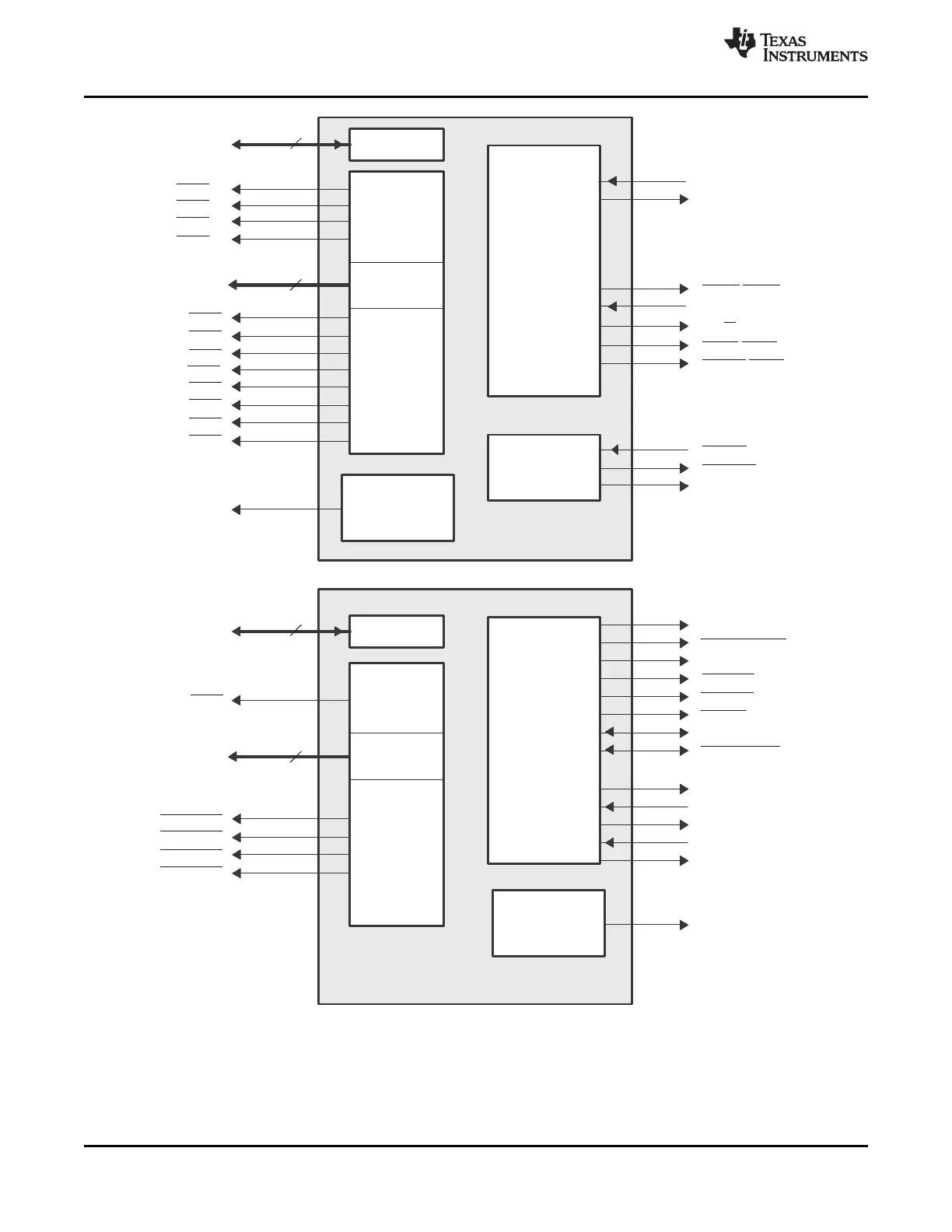
Figure 2-8. EMIFA and DDR2 Memory Controller Peripheral Signals
22 Device Overview Copyright © 2005–2012, Texas Instruments Incorporated
Submit Documentation Feedback
Product Folder Link(s): TMS320C6455

Table of Contents

Other manuals for Texas Instruments TMS320C6455

Question and Answer IconNeed help?

Do you have a question about the Texas Instruments TMS320C6455 and is the answer not in the manual?

Texas Instruments TMS320C6455 Specifications

General IconGeneral
Clock Speed1.0 GHz
Core Count1
On-Chip RAMYes
Data Width32-bit
Data Bus Width64-bit
Operating Voltage1.2 V
I/O Voltage3.3 V
Instruction SetTMS320C64x+
MemoryDDR2
Package TypeBGA
External Memory InterfaceEMIF
InterfacesI2C, SPI

Summary

1 Features

2 Device Overview

2.2 CPU (DSP Core) Description

Details the C64x+ CPU core, functional units, register files, and data paths.

2.4 Boot Sequence

Explains the process of initializing the DSP's memory and registers at reset.

3 Device Configuration

3.1 Device Configuration at Device Reset

Details configuration pins (AEA, ABA, PCI_EN) for boot mode, clock source, and endianness.

5 C64x+ Megamodule

5.1 Memory Architecture

Describes the L2, L1P, and L1D memory configurations and sizes.

6 Device Operating Conditions

6.1 Absolute Maximum Ratings Over Operating Case Temperature Range (Unless Otherwise Noted)

Specifies stress ratings for voltage, temperature, and other conditions beyond which damage may occur.

6.2 Recommended Operating Conditions

Lists recommended operating ranges for supply voltages, input/output, and temperatures.

7 C64x+ Peripheral Information and Electrical Specifications

7.3 Power Supplies

Covers power supply sequencing, decoupling, and power-down operation.

7.4 Enhanced Direct Memory Access (EDMA3) Controller

Details EDMA3 features like transfer dimensions, PaRAM entries, and DMA channels.

7.6 Reset Controller

Describes different reset types (POR, Warm, Max, System, CPU) and their effects.

7.7 PLL1 and PLL1 Controller

Details PLL1 controller operation, clocks, and registers for frequency synthesis.

7.8 PLL2 and PLL2 Controller

Describes PLL2 controller operation, clocks, and registers for EMAC and DDR2 memory.

7.9 DDR2 Memory Controller

Explains DDR2 interface, device-specific information, and memory topologies.

7.10 External Memory Interface A (EMIFA)

Covers EMIFA interface capabilities for various external devices and timing.

7.11 I2C Peripheral

Describes the I2C module, its features, and device-specific information.

7.14 Ethernet MAC (EMAC)

Describes EMAC module, interface modes (MII, RMII, GMII, RGMII), and control modules.

Related product manuals