Memory and bus architecture RM0008
59/1128 DocID13902 Rev 15
Note: For further information on the Flash memory interface registers, please refer to the:
“STM32F10xxx XL-density Flash programming manual” (PM0068) for XL-density devices
“STM32F10xxx Flash programming manual” (PM0075) for other devices
Reading the Flash memory
Flash memory instructions and data access are performed through the AHB bus. The
prefetch block is used for instruction fetches through the ICode bus. Arbitration is performed
in the Flash memory interface, and priority is given to data access on the DCode bus.
Read accesses can be performed with the following configuration options:
• Latency: number of wait states for a read operation programmed on-the-fly
• Prefetch buffer (2 x 64-bit blocks): it is enabled after reset; a whole block can be
replaced with a single read from the Flash memory as the size of the block matches the
bandwidth of the Flash memory. Thanks to the prefetch buffer, faster CPU execution is
possible as the CPU fetches one word at a time with the next word readily available in
the prefetch buffer
• Half cycle: for power optimization
Note: These options should be used in accordance with the Flash memory access time. The wait
states represent the ratio of the SYSCLK (system clock) period to the Flash memory access
time:
zero wait state, if 0 < SYSCLK
≤
24 MHz
one wait state, if 24 MHz < SYSCLK
≤
48 MHz
two wait states, if 48 MHz < SYSCLK
≤
72 MHz
Half cycle configuration is not available in combination with a prescaler on the AHB. The
system clock (SYSCLK) should be equal to the HCLK clock. This feature can therefore be
Flash memory interface
registers
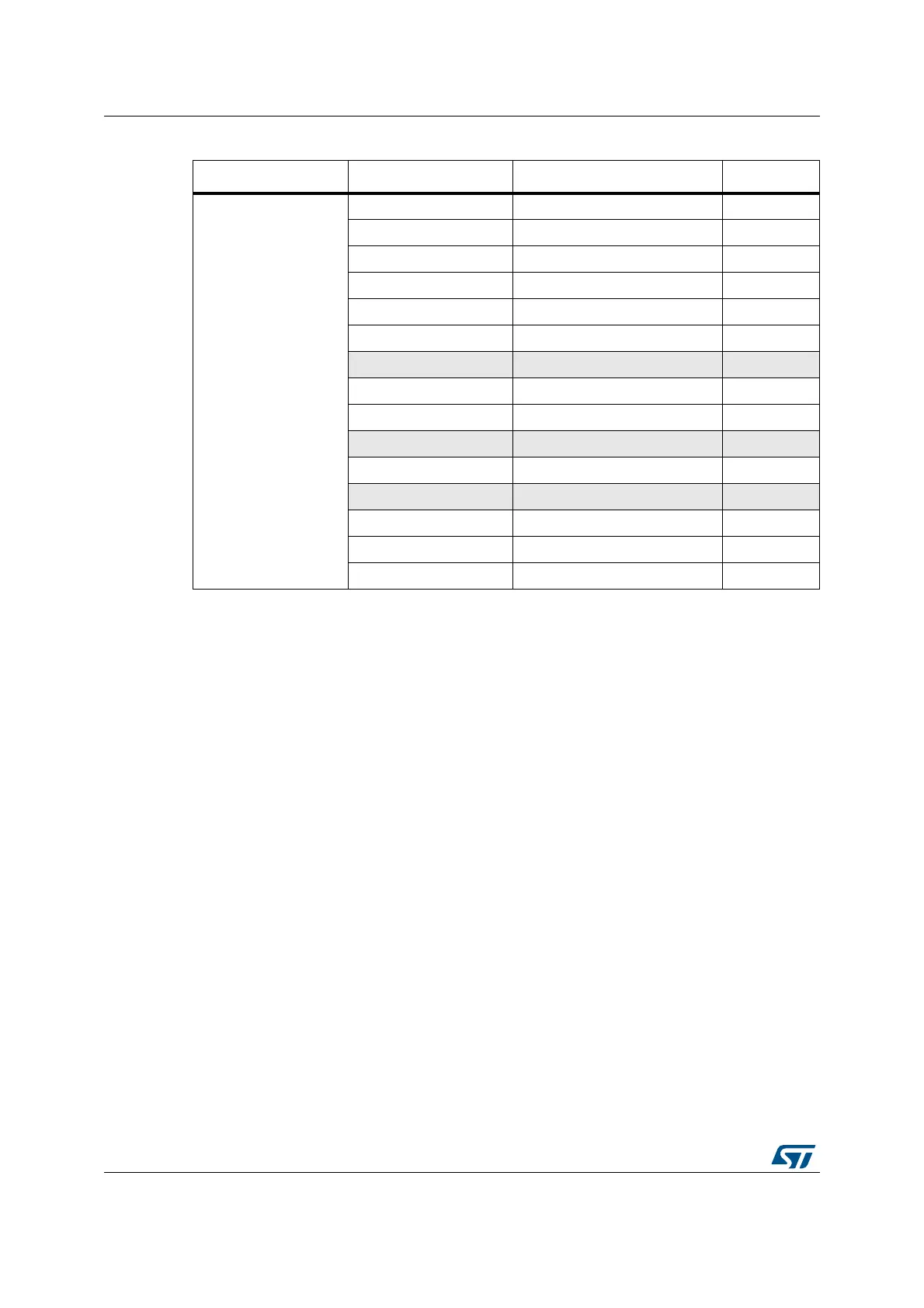
FLASH_ACR 0x4002 2000 - 0x4002 2003 4
FLASH_KEYR 0x4002 2004 - 0x4002 2007 4
FLASH_OPTKEYR 0x4002 2008 - 0x4002 200B 4
FLASH_SR 0x4002 200C - 0x4002 200F 4
FLASH_CR 0x4002 2010 - 0x4002 2013 4
FLASH_AR 0x4002 2014 - 0x4002 2017 4
Reserved 0x4002 2018 - 0x4002 201B 4
FLASH_OBR 0x4002 201C - 0x4002 201F 4
FLASH_WRPR 0x4002 2020 - 0x4002 2023 4
Reserved 0x4002 2024 - 0x4002 2043 32
FLASH_KEYR2 0x4002 2044 - 0x4002 2047 4
Reserved 0x4002 2048 - 0x4002 204B 4
FLASH_SR2 0x4002 204C - 0x4002 204F 4
FLASH_CR2 0x4002 2050 - 0x4002 2053 4
FLASH_AR2 0x4002 2054 - 0x4002 2057 4
Table 8. XL-density Flash module organization (continued)
Block Name Base addresses Size (bytes)
 Loading...


