Embedded Flash memory interface RM0090
108/1731 DocID018909 Rev 11
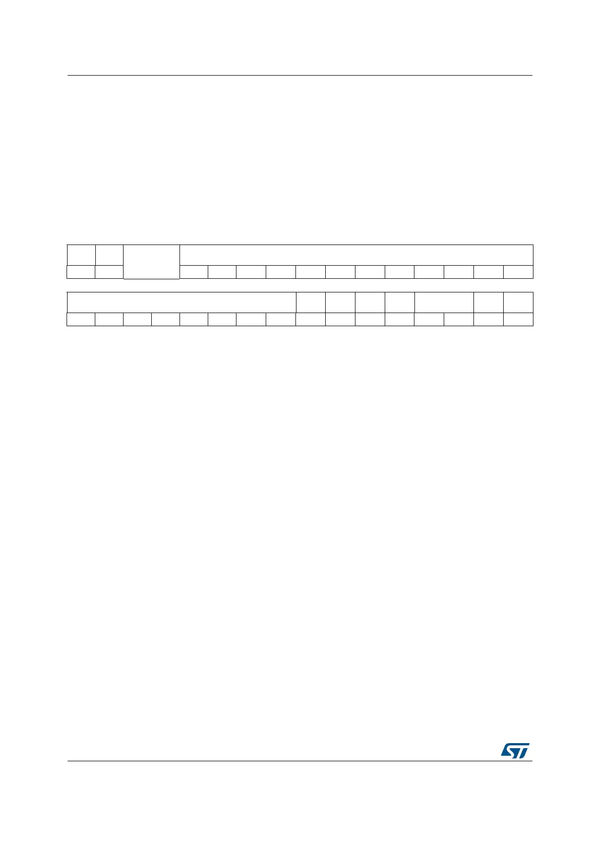
3.9.10 Flash option control register (FLASH_OPTCR)
for STM32F42xxx and STM32F43xxx
The FLASH_OPTCR register is used to modify the user option bytes.
Address offset: 0x14
Reset value: 0x0FFF AAED. The option bits are loaded with values from Flash memory at
reset release.
Access: no wait state when no Flash memory operation is ongoing, word, half-word and
byte access.
31 30 29 28 27 26 25 24 23 22 21 20 19 18 17 16
SPR
MOD
DB1M
Reserved
nWRP[11:0]
rw rw rw rw rw rw rw rw rw rw rw rw rw rw
1514131211109876543210
RDP[7:0]
nRST_
STDBY
nRST_
STOP
WDG_
SW
BFB2 BOR_LEV
OPTST
RT
OPTLO
CK
rw rw rw rw rw rw rw rw rw rw rw rw rw rw rs rs
Bit 31 SPRMOD: Selection of protection mode for nWPRi bits
0: PCROP disabled. nWPRi bits used for Write protection on sector i.
1: PCROP enabled. nWPRi bits used for PCROP protection on sector i
Bit 30 DB1M: Dual-bank on 1 Mbyte Flash memory devices
0: 1 Mbyte single bank Flash memory (contiguous addresses in bank1)
1: 1 Mbyte dual bank Flash memory. The Flash memory is organized as two banks of
512 Kbytes each (see Table 7: 1 Mbyte Flash memory single bank vs dual bank organization
(STM32F42xxx and STM32F43xxx) and Table 9: 1 Mbyte dual bank Flash memory
organization (STM32F42xxx and STM32F43xxx)). To perform an erase operation, the right
sector must be programmed (see Table 7 for information on the sector numbering scheme).
Note: If DB1M is set and an erase operation is performed on Bank 2 while the default sector
number is selected (as an example, sector 8 is configured instead of sector 12), the
erase operation on Bank 2 sector is not performed.
Bits 29:28 Reserved, must be kept cleared.
Bits 27:16 nWRP[11:0]: Not write protect
These bits contain the value of the write-protection and read-protection (PCROP) option bytes
for sectors 0 to 11 after reset. They can be written to program a new write-protect or PCROP
value into Flash memory.
If SPRMOD is reset:
0: Write protection active on sector i
1: Write protection not active on sector i
If SPRMOD is set:
0: PCROP protection not active on sector i
1: PCROP protection active on sector i
Bits 15:8 RDP[7:0]: Read protect
These bits contain the value of the read-protection option level after reset. They can be written
to program a new read protection value into Flash memory.
0xAA: Level 0, read protection not active
0xCC: Level 2, chip read protection active
Others: Level 1, read protection of memories active