General-purpose I/Os (GPIO) RM0090
270/1731 DocID018909 Rev 11
Each I/O port bit is freely programmable, however the I/O port registers have to be
accessed as 32-bit words, half-words or bytes. The purpose of the GPIOx_BSRR register is
to allow atomic read/modify accesses to any of the GPIO registers. In this way, there is no
risk of an IRQ occurring between the read and the modify access.
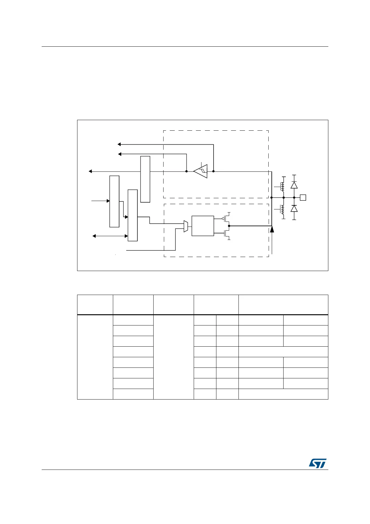
Figure 25 shows the basic structure of a 5 V tolerant I/O port bit. Table 39 gives the possible
port bit configurations.
Figure 25. Basic structure of a five-volt tolerant I/O port bit
1. V
DD_FT
is a potential specific to five-volt tolerant I/Os and different from V
DD
.
Table 35. Port bit configuration table
(1)
MODER(i)
[1:0]
OTYPER(i)
OSPEEDR(i)
[B:A]
PUPDR(i)
[1:0]
I/O configuration
01
0
SPEED
[B:A]
0 0 GP output PP
0 0 1 GP output PP + PU
0 1 0 GP output PP + PD
0 1 1 Reserved
1 0 0 GP output OD
1 0 1 GP output OD + PU
1 1 0 GP output OD + PD
1 1 1 Reserved (GP output OD)
!LTERNATEFUNCTIONOUTPUT
!LTERNATEFUNCTIONINPUT
0USHPULL
OPENDRAINOR
DISABLED
/UTPUTDATAREGISTER
2EADWRITE
&ROMONCHIP
PERIPHERAL
4OONCHIP
PERIPHERAL
/UTPUT
CONTROL
!NALOG
ONOFF
0ULL
0ULL
ONOFF
)/PIN
6
$$
6
$$
6
33
6
33
44,3CHMITT
TRIGGER
6
33
6
$$?&4
0ROTECTION
DIODE
0ROTECTION
DIODE
ONOFF
)NPUTDRIVER
/UTPUTDRIVER
DOWN
UP
0-/3
.-/3
2EAD
"ITSETRESETREGISTERS
7RITE
!NALOG
)NPUTDATAREGISTER
AIB