DMA controller (DMA) RM0090
334/1731 DocID018909 Rev 11
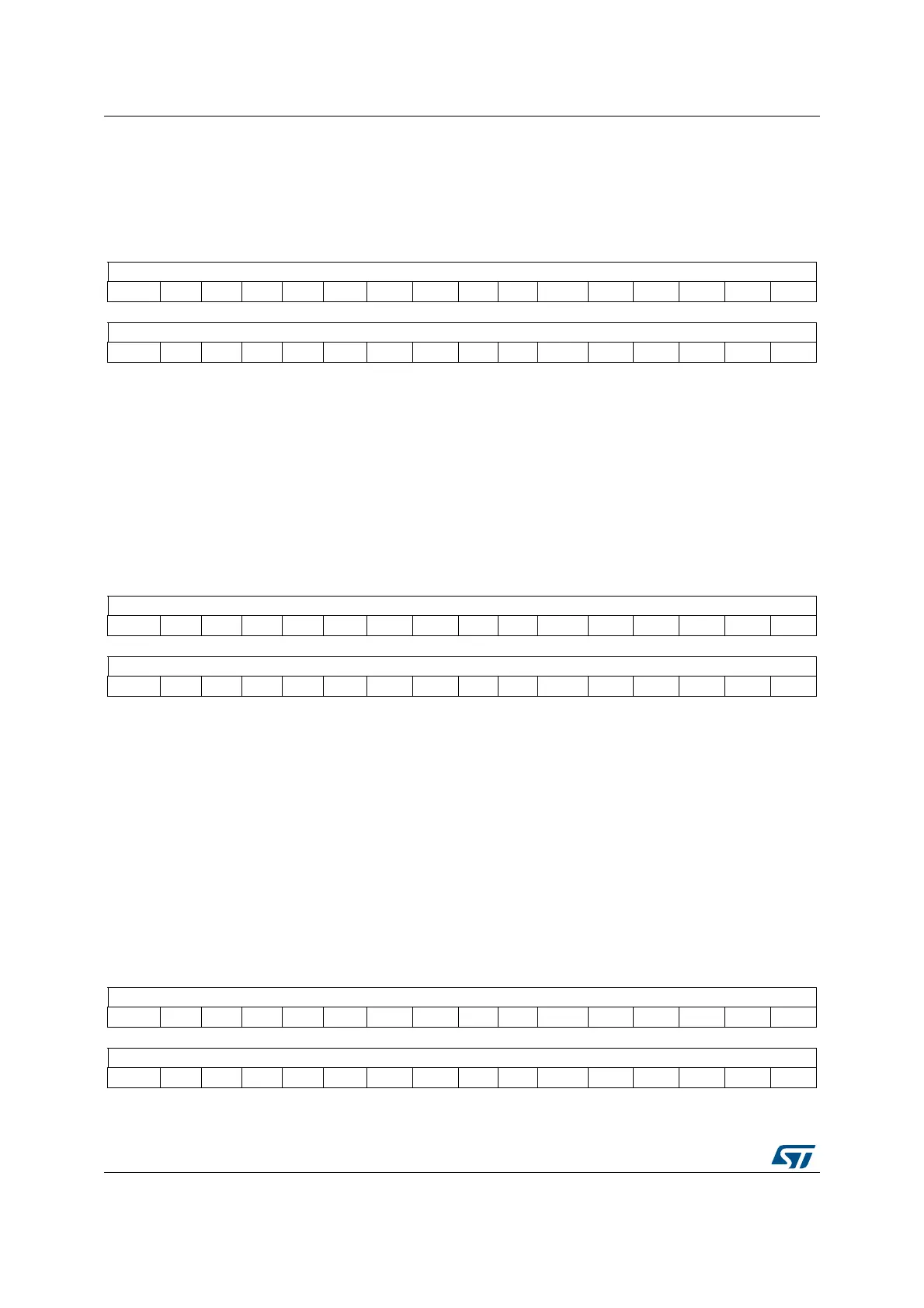
10.5.7 DMA stream x peripheral address register (DMA_SxPAR) (x = 0..7)
Address offset: 0x18 + 0x18 × stream number
Reset value: 0x0000 0000
10.5.8 DMA stream x memory 0 address register (DMA_SxM0AR) (x = 0..7)
Address offset: 0x1C + 0x18 × stream number
Reset value: 0x0000 0000
10.5.9 DMA stream x memory 1 address register (DMA_SxM1AR) (x = 0..7)
Address offset: 0x20 + 0x18 × stream number
Reset value: 0x0000 0000
31 30 29 28 27 26 25 24 23 22 21 20 19 18 17 16
PAR[31:16]
rw rw rw rw rw rw rw rw rw rw rw rw rw rw rw rw
15 14 13 12 11 10 9 8 7 6 5 4 3 2 1 0
PAR[15:0]
rw rw rw rw rw rw rw rw rw rw rw rw rw rw rw rw
Bits 31:0 PAR[31:0]: Peripheral address
Base address of the peripheral data register from/to which the data will be read/written.
These bits are write-protected and can be written only when bit EN = '0' in the DMA_SxCR register.
31 30 29 28 27 26 25 24 23 22 21 20 19 18 17 16
M0A[31:16]
rw rw rw rw rw rw rw rw rw rw rw rw rw rw rw rw
15 14 13 12 11 10 9 8 7 6 5 4 3 2 1 0
M0A[15:0]
rw rw rw rw rw rw rw rw rw rw rw rw rw rw rw rw
Bits 31:0 M0A[31:0]: Memory 0 address
Base address of Memory area 0 from/to which the data will be read/written.
These bits are write-protected. They can be written only if:
– the stream is disabled (bit EN= '0' in the DMA_SxCR register) or
– the stream is enabled (EN=’1’ in DMA_SxCR register) and bit CT = '1' in the
DMA_SxCR register (in Double buffer mode).
31 30 29 28 27 26 25 24 23 22 21 20 19 18 17 16
M1A[31:16]
rw rw rw rw rw rw rw rw rw rw rw rw rw rw rw rw
15 14 13 12 11 10 9 8 7 6 5 4 3 2 1 0
M1A[15:0]
rw rw rw rw rw rw rw rw rw rw rw rw rw rw rw rw