DocID018909 Rev 11 117/1731
RM0090 Power controller (PWR)
149
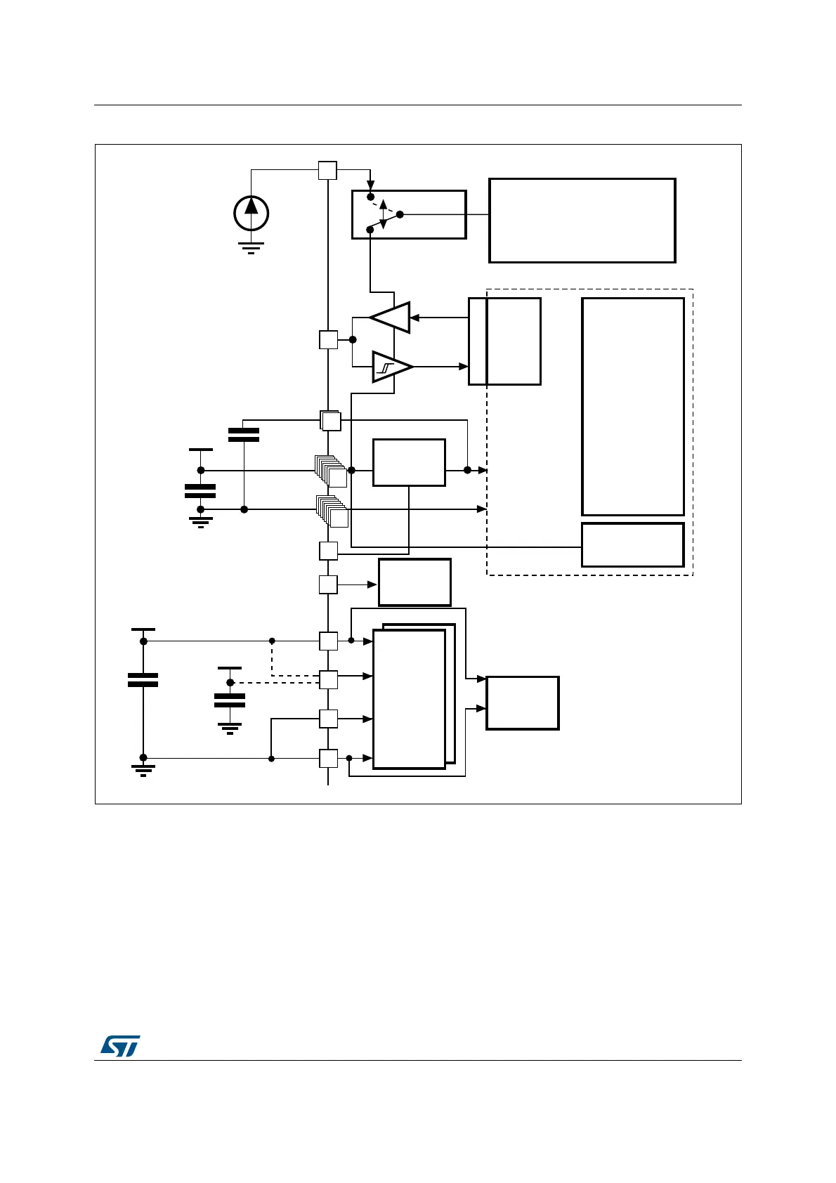
Figure 10. Power supply overview for STM32F42xxx and STM32F43xxx
1. V
DDA
and V
SSA
must be connected to V
DD
and V
SS
, respectively.
5.1.1 Independent A/D converter supply and reference voltage
To improve conversion accuracy, the ADC has an independent power supply which can be
separately filtered and shielded from noise on the PCB.
• The ADC voltage supply input is available on a separate V
DDA
pin.
• An isolated supply ground connection is provided on pin V
SSA
.
To ensure a better accuracy of low voltage inputs, the user can connect a separate external
reference voltage ADC input on V
REF
. The voltage on V
REF
ranges from 1.8 V to V
DDA
.
-36
6
$$
!NALOG
2#S0,,
0OWERSWITCH
6
"!4
'0)/S
/54
).
+ERNELLOGIC
#05
DIGITAL
2!-
"ACKUPCIRCUITRY
/3#+24#
"ACKUPREGISTERS
BACKUP2!-
7AKEUPLOGIC
§N&
§&
6"!4
TO6
6OLTAGE
REGULATOR
6
33
6
$$!
6
2%&
6
2%&
6
33!
!$#
,EVELSHIFTER
)/
,OGIC
6
$$
&
6
2%&
N&
&
6
$$
&LASHMEMORY
6
#!0?
6
#!0?
§&
"90!33?2%'
0$2?/.
2ESET
CONTROLLER
N&