DocID018909 Rev 11 1599/1731
RM0090 Flexible memory controller (FMC)
1669
37.5 NOR Flash/PSRAM controller
The FMC generates the appropriate signal timings to drive the following types of memories:
• Asynchronous SRAM and ROM
–8 bits
– 16 bits
– 32 bits
• PSRAM (Cellular RAM)
– Asynchronous mode
– Burst mode for synchronous accesses
– Multiplexed or non-multiplexed
• NOR Flash memory
– Asynchronous mode
– Burst mode for synchronous accesses
– Multiplexed or non-multiplexed
The FMC outputs a unique Chip Select signal, NE[4:1], per bank. All the other signals
(addresses, data and control) are shared.
The FMC supports a wide range of devices through a programmable timings among which:
• Programmable wait states (up to 15)
• Programmable bus turnaround cycles (up to 15)
• Programmable output enable and write enable delays (up to 15)
• Independent read and write timings and protocol to support the widest variety of
memories and timings
• Programmable continuous clock (FMC_CLK) output.
The FMC Clock (FMC_CLK) is a submultiple of the HCLK clock. It can be delivered to the
selected external device either during synchronous accesses only or during asynchronous
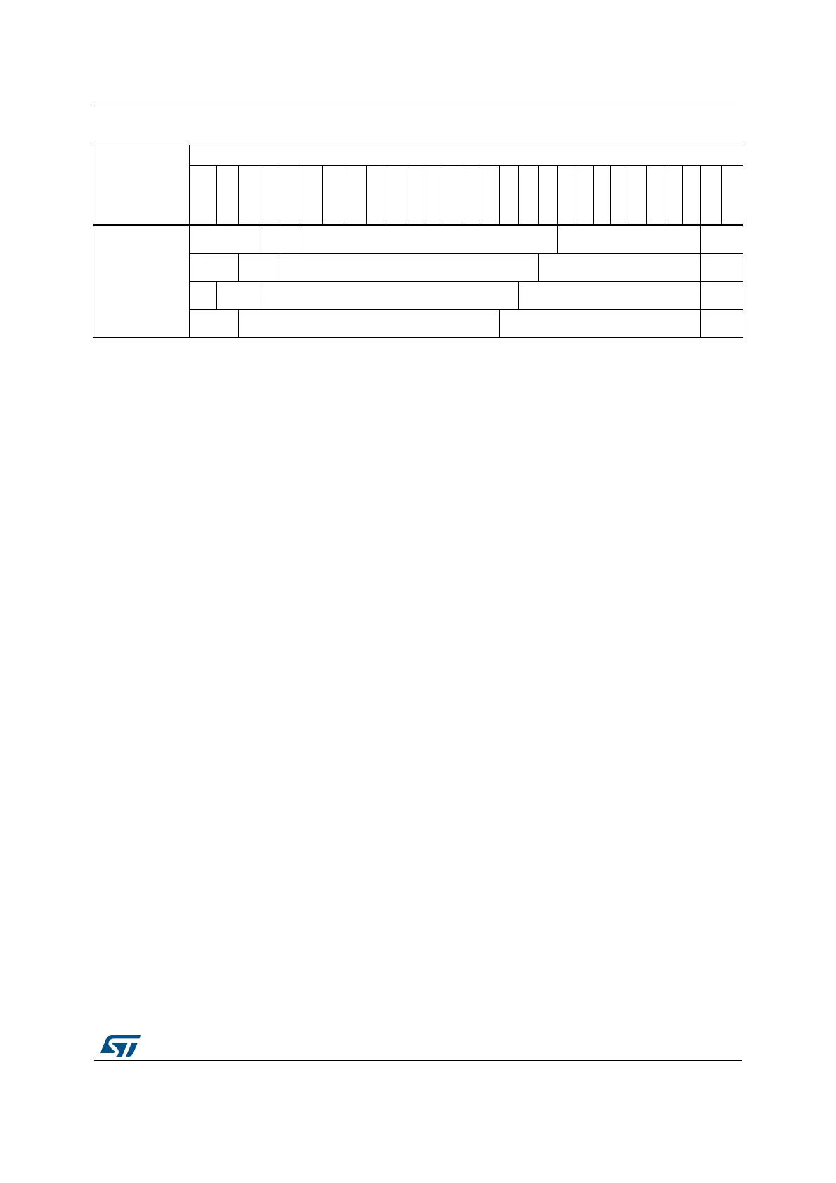
13-bit row size
configuration
Res.
Bank
[1:0]
Row[12:0] Column[7:0] BM[1:0
Res.
Bank
[1:0]
Row[12:0] Column[8:0] BM[1:0
Res.
Bank
[1:0]
Row[12:0] Column[9:0] BM[1:0
Bank
[1:0]
Row[12:0] Column[10:0] BM[1:0
1. BANK[1:0] are the Bank Address BA[1:0]. When only 2 internal banks are used, BA1 must always be set to ‘0’.
2. Access to Reserved space (Res.) generates an AHB error.
3. BM[1:0]: is the byte mask for 32-bit access.
Table 257. SDRAM address mapping with 32-bit data bus width
(1)(2)
(continued)
Row size
configuration
HADDR(AHB address Lines)
27
26
25
24
23
22
21
20
19
18
17
16
15
14
13
12
11
10
9
8
7
6
5
4
3
2
1
0