DocID018909 Rev 11 161/1731
RM0090 Reset and clock control for STM32F42xxx and STM32F43xxx (RCC)
212
6.3 RCC registers
Refer to Section 1.1: List of abbreviations for registers for a list of abbreviations used in
register descriptions.
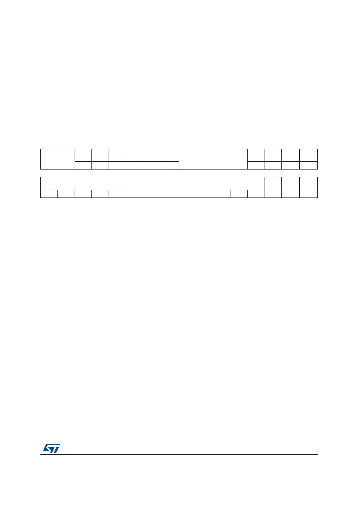
6.3.1 RCC clock control register (RCC_CR)
Address offset: 0x00
Reset value: 0x0000 XX83 where X is undefined.
Access: no wait state, word, half-word and byte access
31 30 29 28 27 26 25 24 23 22 21 20 19 18 17 16
Reserved
PLLSAI
RDY
PLLSAI
ON
PLLI2S
RDY
PLLI2S
ON
PLLRD
Y
PLLON
Reserved
CSS
ON
HSE
BYP
HSE
RDY
HSE
ON
rrwrrwr rw rwrwr rw
15 14 13 12 11 10 9 8 7 6 5 4 3 2 1 0
HSICAL[7:0] HSITRIM[4:0]
Res.
HSI
RDY
HSION
rrrrrrr rrwrwrwrwrw rrw
Bits 31:28 Reserved, must be kept at reset value.
Bit 29 PLLSAIRDY: PLLSAI clock ready flag
Set by hardware to indicate that the PLLSAI is locked.
0: PLLSAI unlocked
1: PLLSAI locked
Bit 28 PLLSAION: PLLSAI enable
Set and cleared by software to enable PLLSAI.
Cleared by hardware when entering Stop or Standby mode.
0: PLLSAI OFF
1: PLLSAI ON
Bit 27 PLLI2SRDY: PLLI2S clock ready flag
Set by hardware to indicate that the PLLI2S is locked.
0: PLLI2S unlocked
1: PLLI2S locked
Bit 26 PLLI2SON: PLLI2S enable
Set and cleared by software to enable PLLI2S.
Cleared by hardware when entering Stop or Standby mode.
0: PLLI2S OFF
1: PLLI2S ON
Bit 25 PLLRDY: Main PLL (PLL) clock ready flag
Set by hardware to indicate that PLL is locked.
0: PLL unlocked
1: PLL locked
Bit 24 PLLON: Main PLL (PLL) enable
Set and cleared by software to enable PLL.
Cleared by hardware when entering Stop or Standby mode. This bit cannot be reset if PLL
clock is used as the system clock.
0: PLL OFF
1: PLL ON