TMS320C6455
www.ti.com
SPRS276M –MAY 2005–REVISED MARCH 2012
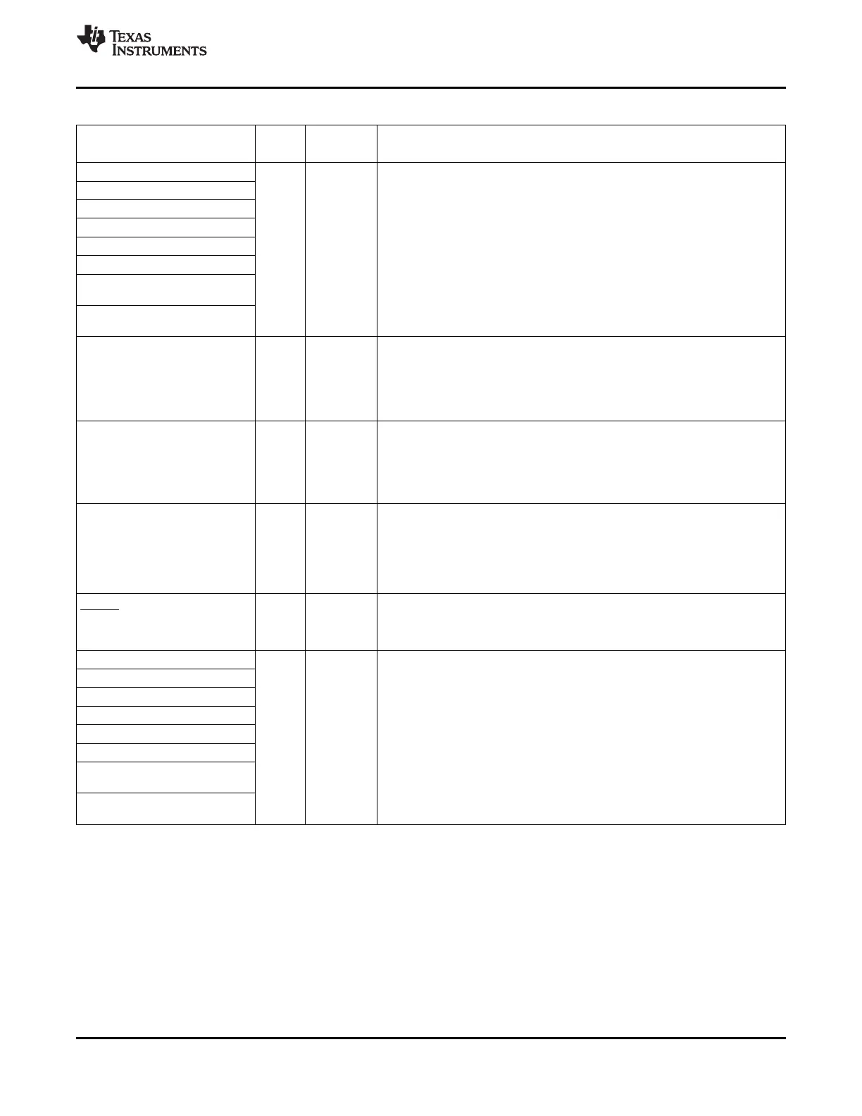
Table 2-3. Terminal Functions (continued)
SIGNAL
TYPE
(1)
IPD/IPU
(2)
DESCRIPTION
NAME NO.
URDATA7/MRXD7 M2
URDATA6/MRXD6 H2
UTOPIA 8-bit Receive Data Bus (I) [default] or EMAC receive data bus for MII
URDATA5/MRXD5 L2
[default], RMII, or GMII
URDATA4/MRXD4 L1
Using the Receive Data Bus, the UTOPIA Slave (on the rising edge of the
URCLK) can receive the 8-bit ATM cell data from the Master ATM Controller.
URDATA3/MRXD3 J3
I
URDATA2/MRXD2 J1
When the UTOPIA peripheral is disabled (UTOPIA_EN [AEA12 pin] = 0), these
pins function as EMAC receive data pins for MII [default], RMII, or GMII
URDATA1/MRXD1/
H3
(MRXD[x:0]) (I). MACSEL[1:0] dependent.
RMRXD1
URDATA0/MRXD0/
J2
RMRXD0
Transmit cell available status output signal from UTOPIA slave (O).
• 0 indicates a complete cell is NOT available for transmit
• 1 indicates a complete cell is available for transmit
UXCLAV/GMTCLK K5 O/Z
When the UTOPIA peripheral is disabled (UTOPIA_EN [AEA12 pin] = 0), this
pin is EMAC GMII transmit clock (GMTCLK) (O). MACSEL[1:0] dependent.
UTOPIA transmit source clock (UXCLK) driven by Master ATM Controller (I) or
when the UTOPIA peripheral is disabled (UTOPIA_EN [AEA12 pin] = 0), this
UXCLK/MTCLK/ pin is either EMAC MII [default] or GMII transmit clock (MTCLK) (I) or the
N4 I
RMREFCLK EMAC RMII reference clock (RMREFCLK) (I). The EMAC function is controlled
by the MACSEL[1:0] (AEA[10:9] pins). For more detailed information, see
Section 3, Device Configuration.
UTOPIA transmit Start-of-Cell signal (O). This signal is output by the UTOPIA
Slave on the rising edge of the UXCLK, indicating that the first valid byte of the
cell is available on the 8-bit Transmit Data Bus (UXDATA[7:0]).
UXSOC/MCOL K3 I/O/Z
When the UTOPIA peripheral is disabled (UTOPIA_EN [AEA12 pin] = 0), this
pin is the EMAC collision sense (MCDL) (I) for MII [default] or GMII.
MACSEL[1:0] dependent.
UTOPIA transmit interface enable input signal [default] (I) or when the UTOPIA
UXENB/ MTXEN/ peripheral is disabled (UTOPIA_EN [AEA12 pin] = 0), this pin is either the
J5 I/O/Z
RMTXEN EMAC transmit enable (MTXEN) (O) for MII [default], RMII, or GMII.
MACSEL[1:0] dependent.
UXDATA7/MTXD7 N5
UXDATA6/MTXD6 M3
UTOPIA 8-bit transmit data bus (O) [default] or
UXDATA5/MTXD5 L5
EMAC transmit data bus for MII [default], RMII, or GMII.
UXDATA4/MTXD4 L3
Using the Transmit Data Bus, the UTOPIA Slave (on the rising edge of the
UXDATA3/MTXD3 K4
O/Z UXCLK) transmits the 8-bit ATM cells to the Master ATM Controller.
UXDATA2/MTXD2 M4
When the UTOPIA peripheral is disabled (UTOPIA_EN [AEA12 pin] = 0), these
UXDATA1/MTXD1/ pins function as EMAC transmit data pins (MTXD[x:0]) (O) for MII, RMII, or
L4
RMTXD1 GMII. MACSEL[1:0] dependent.
UXDATA0/MTXD0/
M1
RMTXD0
Copyright © 2005–2012, Texas Instruments Incorporated Device Overview 39
Submit Documentation Feedback
Product Folder Link(s): TMS320C6455