MC68020/MC68030
PROCESSOR
I H"si iiis"ll I
_l"'rft frfr frfr frfr .-
_ i i ii Efl i
TO
EUS
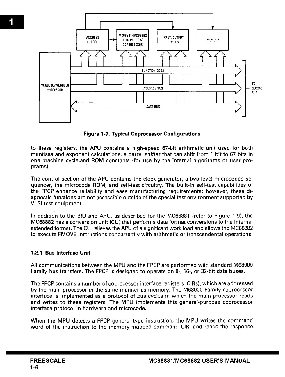
Figure 1-7. Typical Coprocessor Configurations
to these registers, the APU contains a high-speed 67-bit arithmetic unit used for both
mantissa and exponent calculations, a barrel shifter that can shift from 1 bit to 67 bits in
one machine cycle,and ROM constants (for use by the internal algorithms or user pro-
grams).
The control section of the APU contains the clock generator, a two-level microcoded se-
quencer, the microcode ROM, and self-test circuitry. The built-in self-test capabilities of
the FPCP enhance reliability and ease manufacturing requirements; however, these di-
agnostic functions are not accessible outside of the special test environment supported by
VLSI test equipment.
In addition to the BIU and APU, as described for the MC68881 (refer to Figure 1-9), the
MC68882 has a conversion unit (CU) that performs data format conversions to the internal
extended format. The CU relieves the APU of a significant work load and allows the MC68882
to execute FMOVE instructions concurrently with arithmetic or transcendental operations.
1.2.1 Bus Interface Unit
All communications between the MPU and the FPCP are performed with standard M68000
Family bus transfers. The FPCP is designed to operate on 8-, 16-, or 32-bit data buses.
The FPCP contains a number of coprocessor interface registers (CIRs), which are addressed
by the main processor in the same manner as memory. The M68000 Family coprocessor
interface is implemented as a protocol of bus cycles in which the main processor reads
and writes to these registers. The MPU implements this general-purpose coprocessor
interface protocol in hardware and microcode.
When the MPU detects a FPCP general type instruction, the MPU writes the command
word of the instruction to the memory-mapped command CIR, and reads the response
FREESCALE
1-6
MC68881/MC68882 USER'S MANUAL