At9-A13
FCO-FC2
FPCP ACCESS X NON-FPCP ACCESS
A19-AI3
FCO-FC2
i~ NEGATED AT START
,,.~
OF NON-FPCP ACCESS ,, .
(CORRECT)
CS'
A19-AI3
FCO-FC2
DECODE
(X nr, DELAY)
A19-AI3 '~
FPCPACCESS X NON-FPCPACCESS
/ xo, I--
/
ASSERTED DURING
NON-FPCP ACCESS
(INCORRECT)
DECODE
(X ns OELAY)
a) CORRECT Implementation of a "late chip select"
b) INCORRECT Implementation of a "late chip select"
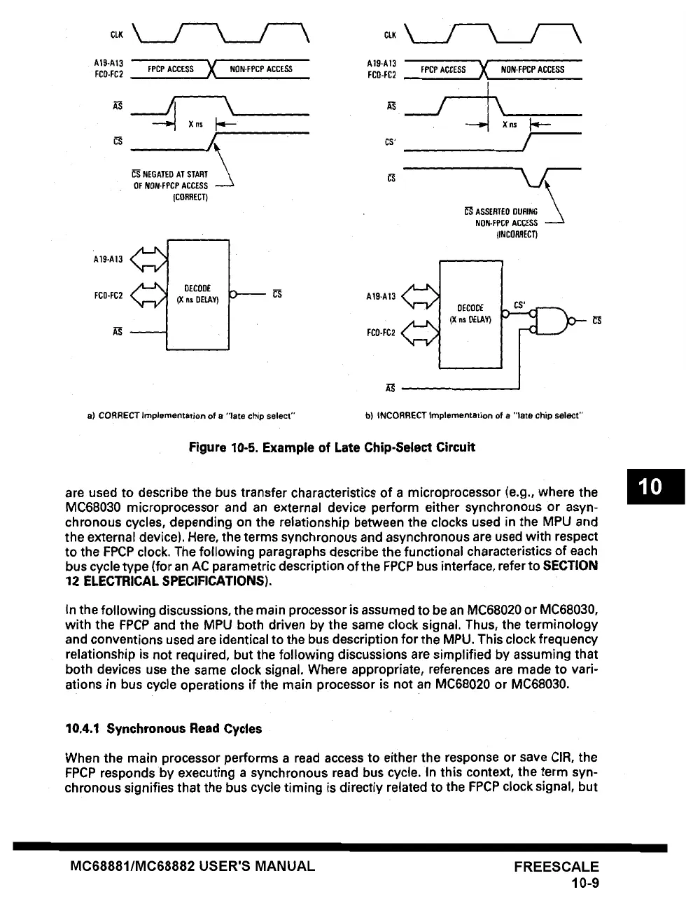
Figure 10-5. Example of Late Chip-Select Circuit
are used to describe the bus transfer characteristics of a microprocessor (e.g., where the
MC68030 microprocessor and an external device perform either synchronous or asyn-
chronous cycles, depending on the relationship between the clocks used in the MPU and
the external device). Here, the terms synchronous and asynchronous are used with respect
to the FPCP clock. The following paragraphs describe the functional characteristics of each
bus cycle type (for an AC parametric description of the FPCP bus interface, refer to SECTION
12
ELECTRICAL SPECIFICATIONS).
In the following discussions, the main processor is assumed to be an MC68020 or MC68030,
with the FPCP and the MPU both driven by the same clock signal. Thus, the terminology
and conventions used are identical to the bus description for the MPU. This clock frequency
relationship is not required, but the following discussions are simplified by assuming that
both devices use the same clock signal. Where appropriate, references are made to vari-
ations in bus cycle operations if the main processor is not an MC68020 or MC68030.
10,4.1 Synchronous Read Cycles
When the main processor performs a read access to either the response or save CIR, the
FPCP responds by executing a synchronous read bus cycle. In this context, the term syn-
chronous signifies that the bus cycle timing is directly related to the FPCP clock signal, but
MC68881/MC68882 USER'S MANUAL FREESCALE
10-9
 Loading...