10
the FPCP clock is not required to be synchronous with the main processor clock during
the transfer• By synchronizing the bus cycle to the FPCP clock, the appropriate response
primitive or format word is always returned based on the current status of the FPCP. Also,
since these bus cycles are used to transmit service requests to the main processor, the
synchronous bus cycle timing allows the main processor and FPCP to be synchronized at
critical points in an instruction dialog, without requiring synchronous clock signals for the
two devices.
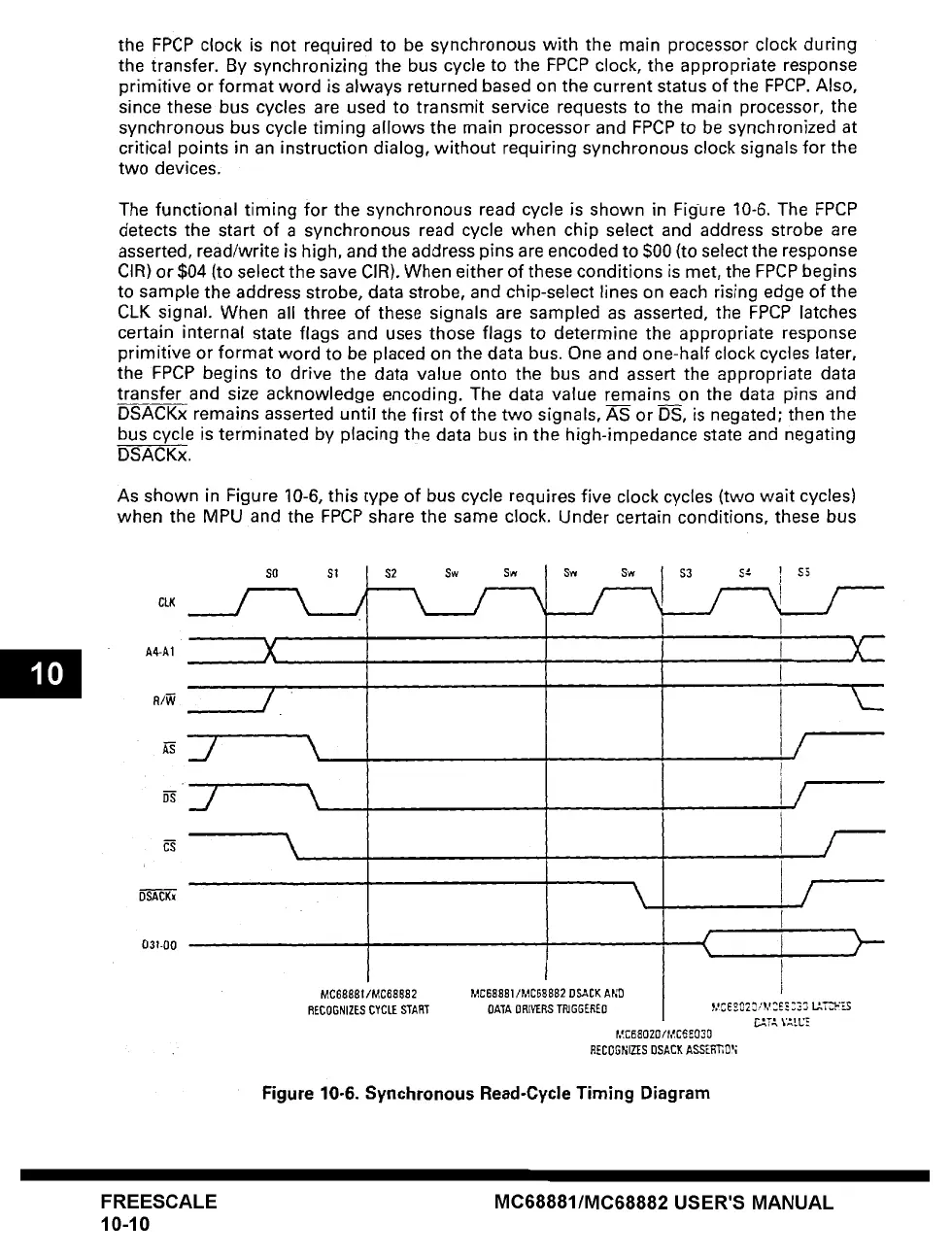
The functional timing for the synchronous read cycle is shown in Figure 10-6. The FPCP
detects the start of a synchronous read cycle when chip select and address strobe are
asserted, read/write is high, and the address pins are encoded to S0O (to select the response
CIR) or $04 (to select the save CIR). When either of these conditions is met, the FPCP begins
to sample the address strobe, data strobe, and chip-select lines on each rising edge of the
CLK signal. When all three of these signals are sampled as asserted, the FPCP latches
certain internal state flags and uses those flags to determine the appropriate response
primitive or format word to be placed on the data bus. One and one-half clock cycles later,
the FPCP begins to drive the data value onto the bus and asser~ the appropriate data
transfer and size acknowledge encoding. The data value remains on the data pins and
DSACKx remains asserted until the first of the two signals, AS or DS, is
negated;
then the
bus cycle is terminated by placing the data bus in the high-impedance state and negating
DSACKx.
As shown in Figure 10-6, this type of bus cycle requires five clock cycles (two wait cycles)
when the MPU and the FPCP share the same clock. Under certain conditions, these bus
CLK
A4-A1
DSACKx
O3l-OO
SO
X
. "
\
\
\
$1 $2
Sw
•
MC68881/MC68B82
RECOGNIZES CYCLE START
Sw
Sw Sw
m
P,,CBBB@|/& C68BB2 DSACK A~D
$3
S~" I S~
I
I
,/
J
/
Id
I
f
, /
.X '
i
DATA DRIVERS TI~GGERED }~;E~0231M~E~331.z,~'T3Z..~':_..S
C~T~ %~tUE
~CES020/~C6E03O
RECOGNIZI[S
OSACK ASSEBI~,0?;
Figure 10-6. Synchronous Read-Cycle Timing Diagram
FREESCALE
10-10
MC68881/MC68882 USER'S MANUAL
 Loading...