As shown in Figure 10-7, this type of bus cycle requires three clock cycles (no wait cycles)
when the MPU and the FPCP share the same clock. Due to the asynchronous timing of the
data transfer and size acknowledge assertion by the FPCP, this bus cycle timing does not
depend on the clock frequency of the FPCP (there are some exceptions to this rule, as
discussed in 10.5 INTER-CYCLE TIMING RESTRICTIONS). For example, if the MC68881
clock frequency is 12.5 MHz and the MPU clock frequency is 16.67 MHZ, this bus cycle
requires three MPU clock cycles since the assertion of DSACKx is recognized by the MPU
on the falling edge of $2. This assumes that the chip-select logic causes the assertion of
A--S and DS so that the AS/DS assertion delay is not lengthened by the chip-select logic
propagation time.
10.4.3 Asynchronous Write Cycles
When the main processor performs any access to the FPCP with RNV low, the FPCP responds
by executing an asynchronous write cycle. The definition of asynchronous in the first
paragraph of the preceding subsection applies also to asynchronous write cycles.
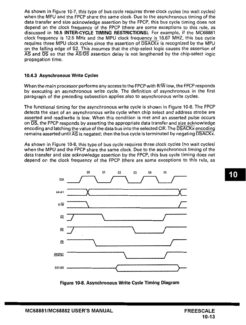
The functional timing for the asynchronous write cycle is shown in Figure 10-8. The FPCP
detects the start of an asynchronous write cycle when chip select and address strobe are
asserted and read/write is low. When this condition is met and an asserted pulse occurs
on D-S, the FPCP responds by asserting the appropriate data transfer and size acknowledge
encoding and latching the value of the data bus into the selected CIR. The DSACKx encoding
remains asserted until AS is negated; then the bus cycle is terminated by negating DSACKx.
As shown in Figure 10-8, this type of bus cycle requires three clock cycles (no wait cycles)
when the MPU and the FPCP share the same clock. Due to the asynchronous timing of the
data transfer and size acknowledge assertion by the FPCP, this bus cycle timing does not
depend on the clock frequency of the FPCP (there are some exceptions to this rule, as
SO $1 $2 $3 $4
$5
/----X /
A4-A1
X
\ /-
=_/ \ /
=_/ \ /
,, ,\ .... /,
DSACY, x
\ /
031-D0
..... >
Figure 10-8. Asynchronous Write Cycle Timing Diagram
MC68881/MC68882 USER'S MANUAL
FREESCALE
10-13