10
When a hardware reset operation is performed, the FPCP immediately aborts any operation
that may have been in progress and returns to the idle state. All of the floating-point data
registers are loaded with nonsignaling NANs, and the FPCR and FPSR are cleared to all
zeros (thus clearing any old status information and selecting the IEEE standard default
operating modes). An identical operation may be performed under software control by a
FRESTORE of a null state frame (although a hardware reset must be executed at power-
up in order to initialize the FPCP).
One consideration that should be given to the ~ signal of the FPCP is the treatment
of a RESET instruction by an M68000 Family processor. When the RESET instruction is
executed by an M68000 Family processor, the internal state of the processor is not affected,
but the external system should respond to the reset operation. Since the FPCP is considered
to be part of the internal state of the main processor, prudent system design suggests that
the FPCP should not respond to the assertion of the ~ signal by the main processor.
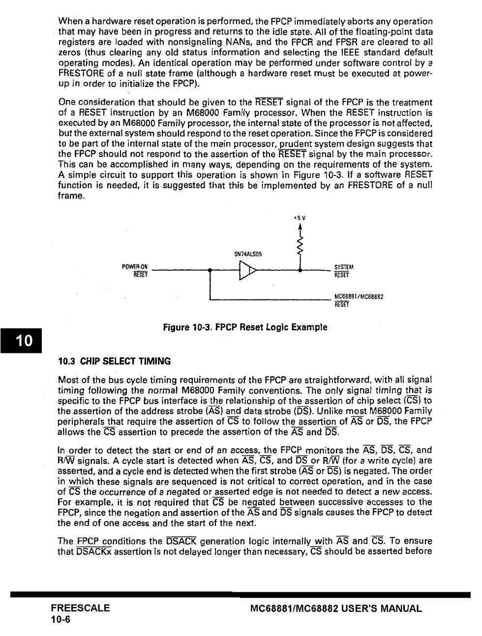
This can be accomplished in many ways, depending on the requirements of the system.
A simple circuit to support this operation is shown in Figure 10-3. If a software RESET
function is needed, it is suggested that this be implemented by an FRESTORE of a null
frame.
+5V
SN7CALSO5 I
P0WER-0N ~ SYSTEM
i msrr
MC68881/MC68882
Figure 10-3. FPCP Reset Logic Example
10.3 CHIP SELECT TIMING
Most of the bus cycle timing requirements of the FPCP are straightforward, with all signal
timing
following the normal M68000 Family conventions. The only signal timing that is
specific to the FPCP bus interface is the relationship of the assertion of chip select (C-S) to
the assertion of the address strobe (AS) and data strobe (DS). Unlike most M68000 Family
peripherals that require the assertion of CS to follow the assertion of A-S or D-S, the FPCP
allows the CS assertion to precede the assertion of the AS and DS.
In order to detect the start or end of an access, the FPCP monitors the AS, DS, CS, and
R/W signals. A cycle start is detected when AS, CS, and D-S or R/W (for a write cycle) are
asserted, and a cycle end is detected when the first strobe (AS or DS) is negated. The order
in which these signals are sequenced is not critical to correct operation, and in the case
of CS the
occurrence of a negated or asserted edge is not needed to detect a new access.
For example, it is not required that C-S be neg__.ated __between successive accesses to the
FPCP, since the negation and assertion of the AS and DS signals causes the FPCP to detect
the end of one access and the start of the next.
The FPCP conditions the DSACK generation logic internally with AS and CS. To ensure
that DSACKx assertion is not delayed longer than necessary, CS should be asserted before
FREESCALE
10-6
MC68881/MC68882 USER'S MANUAL