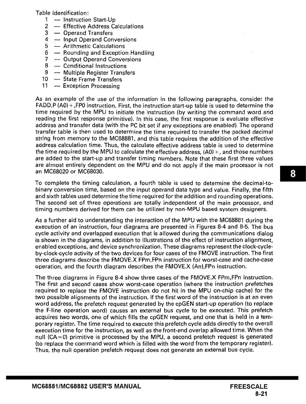
Table
Identification:
1 -- Instruction Start-Up
2 -- Effective Address Calculations
3 -- Operand Transfers
4 -- Input Operand Conversions
5 -- Arithmetic Calculations
6 -- Rounding and Exception Handling
7 ~ Output Operand Conversions
8 -- Conditional Instructions
9 -- Multiple Register Transfers
10 -- State Frame Transfers
11 ~ Exception Processing
As an example of the use of the information in the following paragraphs, consider the
FADD.P (A0) +,FP0 instruction. First, the instruction start-up table is used to determine the
time required by the MPU to initiate the instruction (by writing the command word and
reading the first response primitive). In this case, the first response is evaluate effective
address and transfer data (with the PC bit set if any exceptions are enabled). The operand
transfer table is then used to determine the time required to transfer the packed decimal
string from memory to the MC68881, and this table requires the addition of the effective
address calculation time. Thus, the calculate effective address table is used to determine
the time required by the MPU to
calculate
the effective address, (A0) +, and those numbers
are added to the start-up and transfer timing numbers. Note that these first three values
are almost entirely dependent on the MPU and do not apply if the main processor is not
an MC68020 or MC68030.
To complete the timing calculation, a fourth table is used to determine the decimal-to-
binary conversion time, based on the input operand data type and value. Finally, the fifth
and sixth tables used determine the time required for the addition and rounding operations.
The second set of three operations are totally independent of the main processor, and
timing numbers derived for them can be utilized by non-MPU based system designers.
As a further aid to understanding the interaction of the MPU with the MC68881 during the
execution of an instruction, four diagrams are presented in Figures 8-4 and 8-5. The bus
cycle activity and overlapped execution that is allowed during the communications dialog
is shown in the diagrams, in addition to illustrations of the effect of instruction alignment,
enabled exceptions, and device synchronization. These diagrams represent the clock-cycle-
by-clock-cycle activity of the two devices for four cases of the FMOVE instruction. The first
three diagrams describe the FMOVE.X FPm,FPn instruction for worst-case and cache-case
operation, and the fourth diagram describes the FMOVE.X (An),FPn instruction.
The three diagrams in Figure 8-4 show three cases of the FMOVE.X FPm,FPn instruction.
The first and second cases show worst-case operation (where the instruction prefetches
required to
replace
the FMOVE instruction do not hit in the MPU on-chip cache) for the
two possible alignments of the instruction. If the first word of the instruction is at an even
word address, the prefetch request generated by the cpGEN start-up operation (to replace
the F-line operation word) causes an external bus cycle to be executed. This prefetch
acquires two words, one of which fills the cpGEN request, and one that is held in a tem-
porary register. The time required to execute this prefetch cycle adds directly to the overall
execution time for the instruction, as well as the front-end overlap allowed time. When the
null (CA=0) primitive is processed by the MPU, a second prefetch request is generated
(to replace the command word which is filled with the word from the temporary register).
Thus, the null operation prefetch request does not generate an external bus cycle.
MC68881/MC68882 USER'S MANUAL FREESCALE
8-21
 Loading...