8
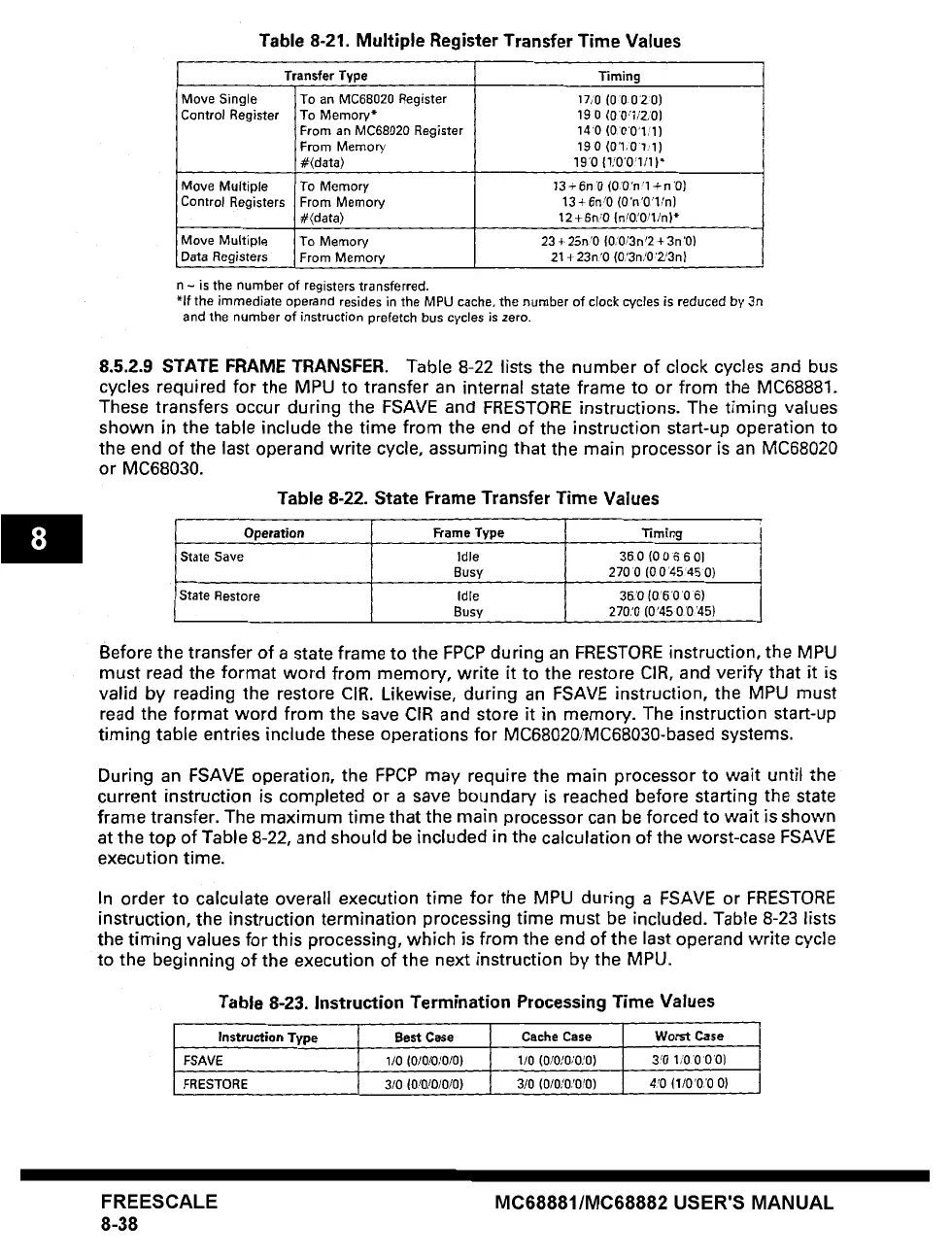
Table 8-21. Multiple Register Transfer Time Values
Transfer
Type Timing
Move Single To an MC68020 Register 17/0 (0'00'20)
Control Register To Memory* 19 0 (00"I/Z0)
From an MC68020 Register 140 (0'0'0'1/1)
From Memory 19 0 (0'1,0'1,1)
#(data) 19'0 {lf0'01/1)*
Move Multiple To Memory 13+6n'0 (0'0'n'l ÷n'0)
Control Registers From Memory 13+6n,'0 (0'n'O'l!n)
#<data) 12 + 6n;0
{n/O,'O!l/n)*
Move Multiple To Memory 23 +25n/0 (0/0/3n'2+3n'0)
Data
Registers From Memory 21 +23n~0 (0!3n/0~2J3n}
n - is the number of registers transferred.
*if the immediate operand resides in the MPU cache, the number of clock cycles is reduced by 3n
and the number of instruction prefetch bus cycles is zero,
8.5.2.9
STATE FRAME
TRANSFER. Table 8-22 lists the number of clock cycles and bus
cycles required for the MPU to transfer an internal state frame to or from the MC68881.
These transfers occur during the FSAVE and FRESTORE instructions. The timing values
shown in the table include the time from the end of the instruction start-up operation to
the end of the last operand write cycle, assuming that the main processor is an MC68020
or MC68030.
Table 8-22. State Frame Transfer Time Values
Operation Frame Type Timing
State Save Idle 360 (0 0 6 6 01
Busy 270 0 (0 0'45'450)
State Restore Idle
Busy
35/0 (0'6'0 '0 6)
270'0 (0'45 0"0 '45)
Before the transfer of a state frame to the FPCP during an FRESTORE instruction, the MPU
must read the format word from memory, write it to the restore CIR, and verify that it is
valid by reading the restore CIR. Likewise, during an FSAVE instruction, the MPU must
read the format word from the save CIR and store it in memory. The instruction start-up
timing table entries include these operations for MC68020/MC68030-based systems.
During an FSAVE operation, the FPCP may require the main processor to wait until the
current instruction is completed or a save boundary is reached before starting the state
frame transfer. The maximum time that the main processor can be forced to wait is shown
at the top of Table 8-22, and should be included in the calculation of the worst-case FSAVE
execution time.
In order to calculate overall execution time for the MPU during a FSAVE or FRESTORE
instruction, the instruction termination processing time must be included. Table 8-23 lists
the timing values for this processing, which is from the end of the last operand write cycle
to the beginning of the execution of the next instruction by the MPU.
Table 8-23. Instruction Termination Processing Time Values
Instruction Type Best Case Cache Case Worst Case
FSAVE 1/0 (0J0/0/0/0) 1/0 (0/0/0/0,'0) 3~0 1/0'00 0)
FRESTORE 3t0
(010]010/0)
310
(0/0,'0,'0,'0)
4'0 (I/0'0'0 O)
FREESCALE
8-38
MC68881/MC68882 USER'S MANUAL
 Loading...