Table 8-20. Conditional Termination Times Values
Best Case Cache Case Worst Case
6/0 (0/0/0/0/0) 6/0 (0/0/0/0/0) 9/0 (2/0/0/0/0)
4/0 (0/0/0/0/0) 4/0 (0/0/0/0/0) 5/0 (I/0/0/0/0)
6/0 (0/0/0/0/0) 6t0 (0f0/0t0/0) 910 (2/010/0)0)
4/0
(0/010/0/0)
4/0 (0/0/0/0/0) 7/0
(2/0/0/0/0)
6/0
(0/0/0/0/0)
6/0 (0/0/0/0/0) 7/0
(1/0/0/0/0)
10/0 (0/0/0/0/0) 10/0
(0/0/0/0/0)
15/0 (3/0/0/0/0)
6/0 (0/0/0/0/0) 6/0 (0/0/0/0/0) 9/0 (2/0/0/0/0)
4/0 (0/0/0/0/0) 4/0
(0/0/0/0/0)
4/0 (1/0/0/0/0)
6/0
(0/0/1/0/0(
810 (0/0/1/0/0) 8/0
(110tl/0/0)
4/0 (0/0/1/0/0) 6/0 (0/0/1/0/0/} 6/0 (1/0/1/0/0)
FTRAPcc 24/0 (0/1/4/0/0) 25/0 (0/1/4/0/0) 30/0 (2/1/4/0/0}
4/0
(0/0/0/0/0)
4/0 (0/0/0/0/0) 5/0 (1/0/0/0/0)
FTRAPcc.W 26/0 (0/114/010) 27/0 (0/1/4/0/0) 28/0
(211/4/0/0)
6/0
(0t0/0t010}
6/0 (0/0/0/0/0) 6f0 (1/0/0/0/0)
FTRAPcc.L
Instruction
Type
FBcc.W Branch Taken
Branch Not Taken
FBcc.L Branch Taken
Branch Not Taken
FDScc True, Not Taken
IFa se, Not Taken
False, Taken
FScc Dn
IAn) + or- (An)*
Memory**
Trap Taken
Trap Not Taken
Trap Taken
Trap Not Taken
Trap Taken
Trap Not Taken
2810
(011/4/0/0)
8/0 (0/0/0/0/0)
29/0
(0/1/4/0/0)
8t0 {0/0/0/010)
*For condition true; subtract one clock for condition false.
**Add the appropriate effective address calculation time.
35/0 (3/1/4/0/0)
10/0 (210t01010)
are used in a system, the execution of other coprocessors may overlap with the execution
of these instructions.
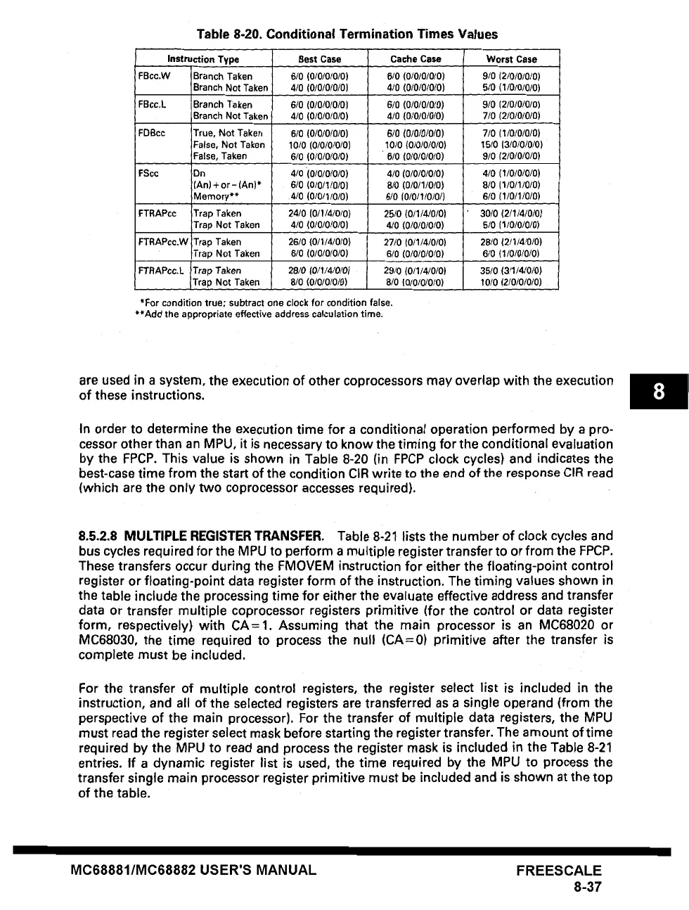
In order to determine the execution time for a conditional operation performed by a pro-
cessor other than an MPU, it is necessary to know the timing for the conditional evaluation
by the FPCP. This value is shown in Table 8-20 (in FPCP clock cycles) and indicates the
best-case time from the start of the condition CIR write to the end of the response CIR read
(which are the only two coprocessor accesses required).
8.5.2.8 MULTIPLE REGISTER TRANSFER. Table 8-21 lists the number of clock cycles and
bus cycles required for the MPU to perform a multiple register transfer to or from the FPCP.
These transfers occur during the FMOVEM instruction for either the floating-point control
register or floating-point data register form of the instruction. The timing values shown in
the table include the processing time for either the evaluate effective address and transfer
data or transfer multiple coprocessor registers primitive (for the control or data register
form, respectively) with CA=I. Assuming that the main processor is an MC68020 or
MC68030, the time required to process the null (CA=0) primitive after the transfer is
complete must be included.
For the transfer of multiple control registers, the register select list is included in the
instruction, and all of the selected registers are transferred as a single operand (from the
perspective of the main processor). For the transfer of multiple data registers, the MPU
must read the register select mask before starting the register transfer. The amount of time
required by the MPU to read and process the register mask is included in the Table
8-21
entries. If a dynamic register list is used, the time required by the MPU to process the
transfer single main processor register primitive must be included and is shown at the top
of the table.
MC68881/MC68882 USER'S MANUAL FREESCALE
8-37