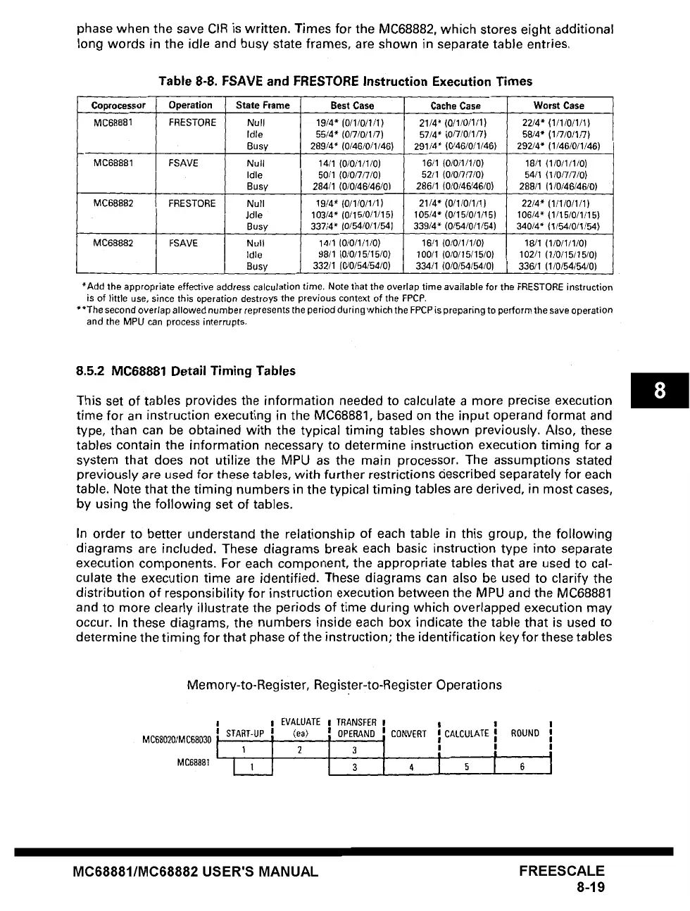
phase when the save CIR is written. Times for the MC68882, which stores eight additional
long words in the idle and busy state frames, are shown in separate table entries.
Table 8-8. FSAVE and FRESTORE Instruction Execution Times
Coprocessor Operation State Frame Best Case Cache Case Worst Case
MC68881 FRESTORE Null 19/4" (0/1/0/1/1) 21/4" (0/1/0/1/1) 22/4* (1/1/0/1/1)
Idle 55/4* (0/7/0/1/7) 5714" (0/7/0/1/7) 58/4* (1/7t0/1/7)
Busy 289/4* (0/46/0/1/46) 291/4" (0/46/0/1/46) 292/4* (1/46/0/1/46)
MC68881 FSAVE Null 14/1 (0/0/1/1/0) 16/1 (0/0/1/1/0) 18/I (1/0/1/1/0)
Idle 50/1 (0/0/7/7/0) 52/1 (0/0/7/7/0) 54/1 (I/0/7/7/0}
Busy 284/1 (0/0/46/46/0) 286/1 (0/0/46/46/0) 288/1 (1/0/46/46/0)
MC68882 FRESTORE Null 19,/4" (0/1/0/1/1) 21/4" (0/1/0/1/I) 22/4* (1/1/0/1/1)
Jdle 103/4" (0/15/0/1/15) 105/4" (0/15/0/1/15) 106/4" (1/15/0/1/15)
Busy 337/4* (0/54/0/1/54} 339/4* (0/54/0/1/54) 340/4*
(1t54/0/I/54)
MC68882 FSAVE Null 1411 (0/0/1/1/0) 15/1 (0/0/1/1/0) 18/1 (1/0/1/1/0)
Idle 98/1 (0/0/15/15/0) 100/1 (010/15/15/0) 102/1 (1/0/15/15/0)
Busy 332/1 (0/0/54/54/0) 334/1 (0/0/54/54/0) 336/1 (1/0/54/54/0)
*Add the appropriate effective address calculation time. Note that the overlap time available for the FRESTORE instruction
is of little use, since this operation destroys the previous context of the FPCP.
**The second overlap allowed number represents the period duri ng which the FPCP is preparing to perform the
save
operation
and the MPU can process interrupts,
8.5.2 MC68881 Detail Timing Tables
This set of tables provides the information needed to calculate a more precise execution
time for an instruction executing in the MC68881, based on the input operand format and
type, than can be obtained with the typical timing tables shown previously. Also, these
tables contain the information necessary to determine instruction execution timing for a
system that does not utilize the MPU as the main processor. The assumptions stated
previously
are
used for these tables, with further restrictions described separately for each
table. Note that the timing numbers in the typical timing tables are derived, in most cases,
by using the following set of tables.
In order to better understand the relationship of each table in this group, the following
diagrams are included. These diagrams break each basic instruction type into separate
execution components. For each component, the appropriate tables that are used to cal-
culate the execution time are identified. These diagrams can also be used to clarify the
distribution of responsibility for instruction execution between the MPU and the MC68881
and to more clearly illustrate the periods of time during which overlapped execution may
occur. In these diagrams, the numbers inside each box indicate the table that is used
to
determine the timing for that phase of the instruction; the identification key for these tables
Memory-to-Register, Register-to-Register Operations
MC68020/MC68030
MC68881
I I EVALUATE I TRANSFER I I I I
I 1 3 4 5 6
MC68881/MC68882 USER'S MANUAL FREESCALE
8-19
 Loading...