9
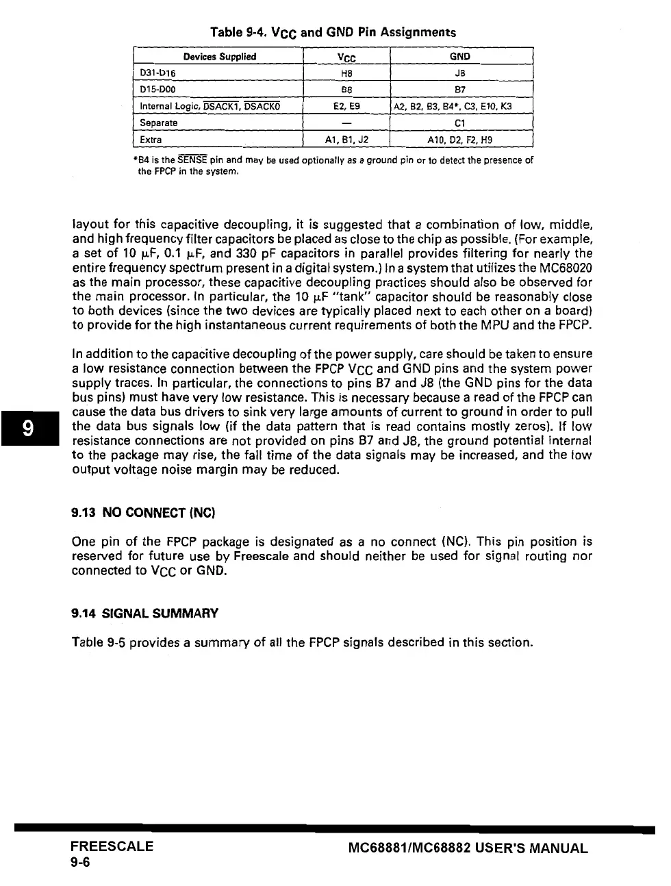
Table 9-4. VCC and GND Pin Assignments
Devices
Supplied
D31-D16
D15-D00
Vcc
GND
H8 J8
B8
87
Internal Logic, DSACK1, DSACK0 E2, E9 A2, B2, B3, B4*, C3, El0, K3
Separate -- C1
Extra A1, B1, J2 A10, D2, F2, H9
*B4 is the SENSE pin and may be used optionally as a ground pin or to detect the presence of
the FPCP in the system.
layout for this capacitive decoupling, it is suggested that a combination of low, middle,
and high frequency filter capacitors be placed as close to the chip as possible. (For example,
a set of 10 ~F, 0.1 ~F, and 330 pF capacitors in parallel provides filtering for nearly the
entire frequency spectrum present in a digital system.) In a system that utilizes the MC68020
as the main processor, these capacitive decoupling practices should also be observed for
the main processor. In particular, the 10 I~F "tank" capacitor should be reasonably close
to both devices (since the two devices are typically placed next to each other on a board)
to provide for the high instantaneous current requirements of both the MPU and the FPCP.
In addition to the capacitive decoupling of the power supply, care should be taken to ensure
a low resistance connection between the FPCP VCC and GND pins and the system power
supply traces. In particular, the connections to pins B7 and J8 (the GND pins for the data
bus pins) must have very low resistance. This is necessary because a read of the FPCP can
cause the data bus drivers to sink very large amounts of current to ground in order to pull
the data bus signals low (if the data pattern that is read contains mostly zeros). If low
resistance connections are not provided on pins B7 and J8, the ground potential internal
to the package may rise, the fall time of the data signals may be increased, and the low
output voltage noise margin may be reduced.
9.13 NO CONNECT (NC)
One pin of the FPCP package is designated as a no connect (NC). This pin position is
reserved for future use by Freescale and should neither be used for signal routing nor
connected to VCC or GND.
9.14 SIGNAL SUMMARY
Table 9-5 provides a summary of all the FPCP signals described in this section.
FREESCALE
9-6
MC68881/MC68882 USER'S MANUAL