9
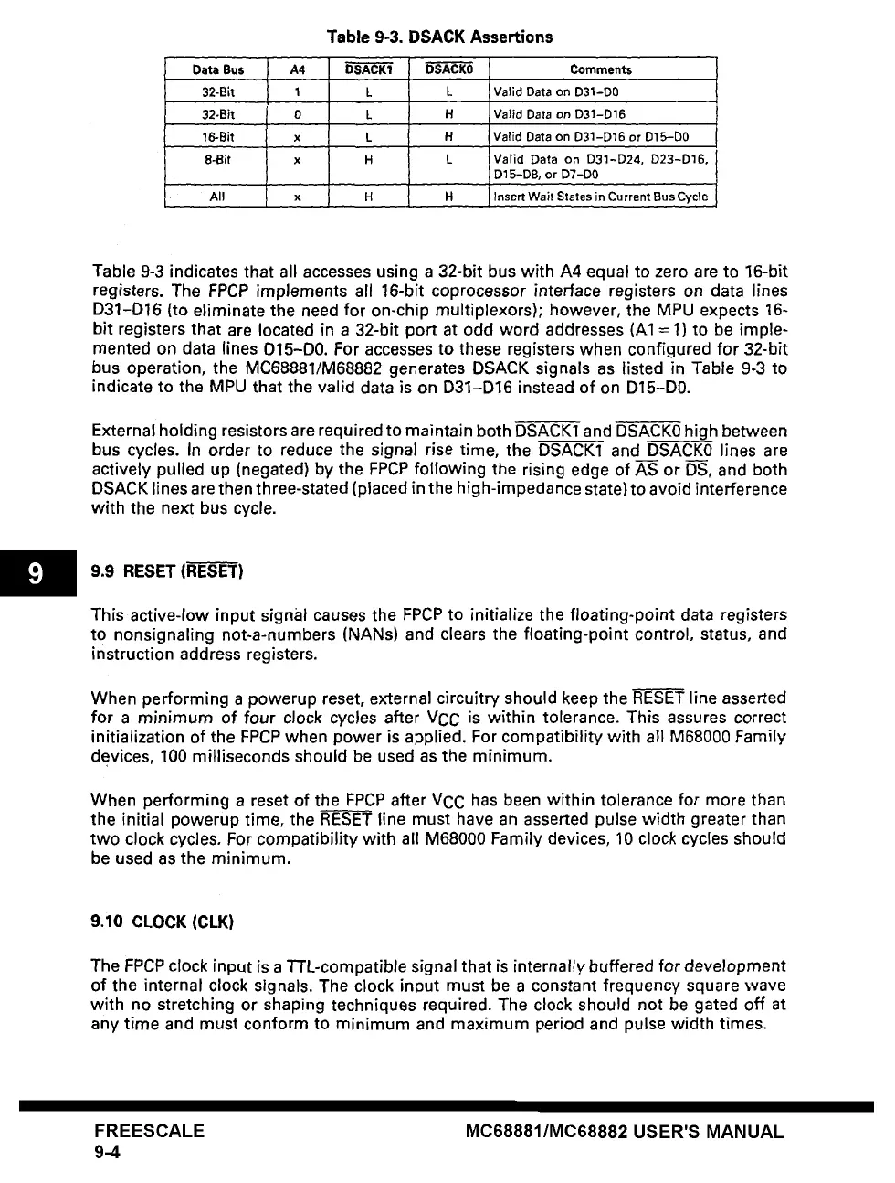
Data Bus A4
32-Bit 1
32-Bit 0
16-Bit x
8-Bit x
All x
Table 9-3. DSACK Assertions
DSACK0 Comments
L L Valid Data on D31-D0
L H Valid
Data
on D31-D16
L H Valid Data on D31-D16 or D15-D0
H L Valid Data on D31-D24, D23-D16,
D15-DS, or D7-D0
H H Insert Wait States in Current Bus Cycle
Table 9-3 indicates that all accesses using a 32-bit bus with A4 equal to zero are to 16-bit
registers. The FPCP implements all 16-bit coprocessor interface registers on data lines
D31-D16 (to eliminate the need for on-chip multiplexors); however, the MPU expects 16-
bit registers that are located in a 32-bit port at odd word addresses (A1 = 1} to be imple-
mented on data lines 015-D0. For accesses to these registers when configured for 32-bit
bus operation, the MC68881/M68882 generates DSACK signals as listed in Table 9-3 to
indicate to the MPU that the valid data is on D31-D16 instead of on D15-D0.
External holding resistors are required to maintain both DSACK1 and DSACK0 high between
bus cycles. In order to reduce the signal rise time, the DSACK1 and DSACK0 lines are
actively pulled up (negated) by the FPCP following the rising edge of AS or DS, and both
DSACK lines are then three-stated (placed in the high-impedance state) to avoid interference
with the next bus cycle.
9.9 RESET (R---E'S~)
This active-low input signal causes the FPCP to initialize the floating-point
data
registers
to nonsignaling not-a-numbers (NANs) and clears the floating-point control, status, and
instruction address registers.
When performing a powerup reset, external circuitry should keep the RESET line asserted
for a minimum of four clock cycles after VCC is within tolerance. This assures correct
initialization of the FPCP when power is applied. For compatibility with all M68000 Family
devices, 100 milliseconds should be used as the minimum.
When performing a reset of the FPCP after VCC has been within tolerance for more than
the initial powerup time, the ~ line must have an asserted pulse width greater than
two clock cycles. For compatibility with all M68000 Family devices, 10 clock cycles should
be used as the minimum.
9.10 CLOCK (CLK)
The FPCP clock input is a TTL-compatible signal that is internally buffered for development
of the internal clock signals. The clock input must be a constant frequency square wave
with no stretching or shaping techniques required. The clock should not be gated off at
any time and must conform to minimum and maximum period and pulse width times.
FREESCALE
9-4
MC68881/MC68882 USER'S MANUAL
 Loading...