DL205 Analog Manual, 7th Edition Rev. D
14-20
Chapter 14: F2-4AD2DA, 4-Ch. In / 2-Ch. Out Analog Combination
1
2
3
4
5
6
7
8
9
10
11
12
13
14
A
B
C
DD
C
b
A
14
13
12
11
10
9
8
7
6
5
4
3
2
1
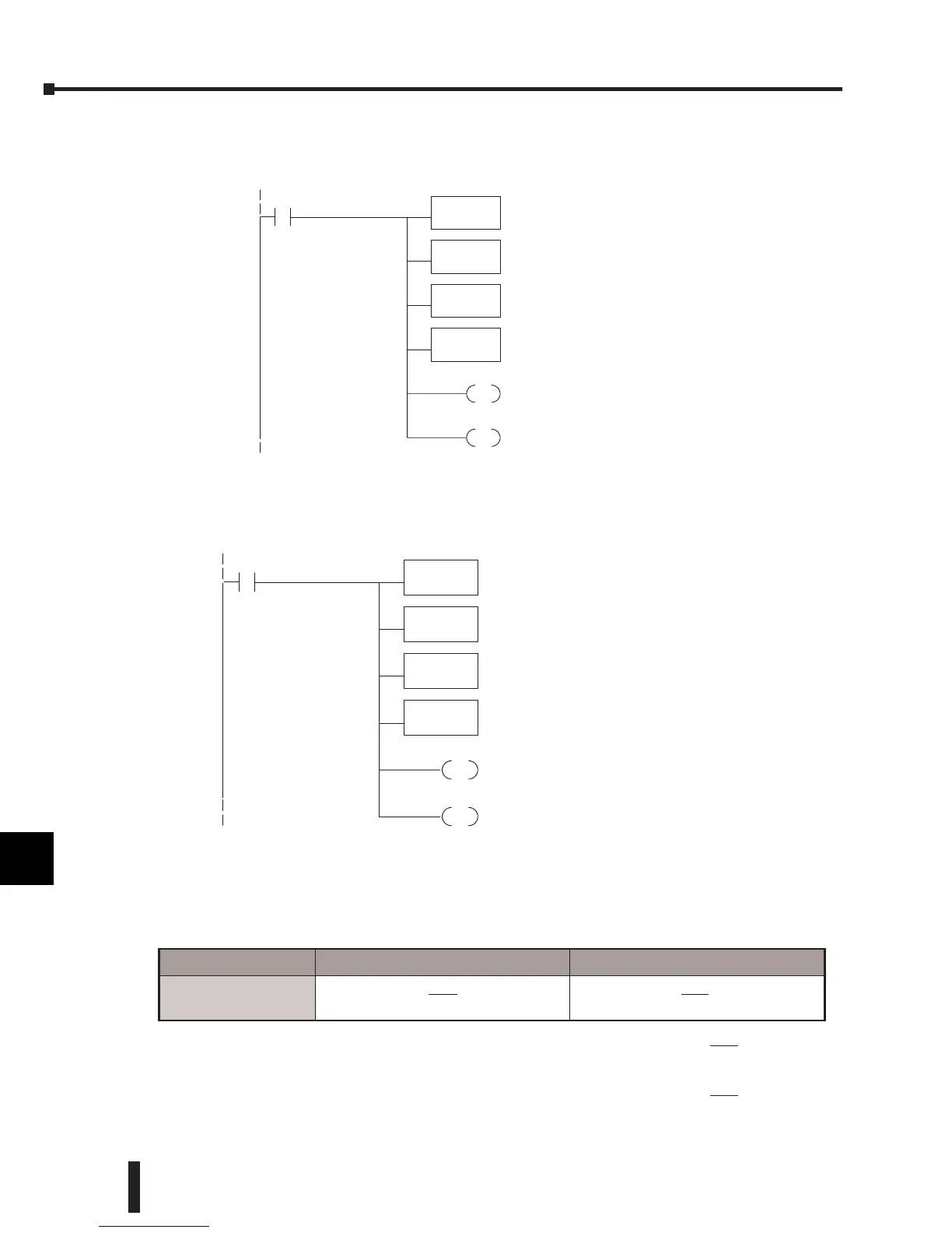
Write Data to One Channel
If only one channel is being used, or if the updates are to be controlled separately, the following
logic can be used.
Write the same Data to Both Channels
If both channel select outputs are Off, then both channels will be updated with the same data.
Analog and Digital Value Conversions
It is sometimes useful to do quick conversions between the signal levels and the digital values.
This can be helpful during startup and/or troubleshooting. The following table shows some
formulas to help with the conversions.
For example, if a 10mA signal level is needed, use the
formula to the right to determine the digital value “D” to
be stored in the V-memory location which is designated to
store the data.
Range If the digital value is known If the analog signal level is known.
4 – 20 mA
A =
16D + 4
4095
D =
4095
(A – 4)
16
BIN
SP1
LD
V2000
OUT
V40501
TheLD instruction loadsthe data intothe
accumulator.Since SP1 is used, this rung
automatically executes on every scan. Youcould
alsouse an X, C, etc. permissive contact.
TheBIN instruction converts theaccumulator data
to binary (you must omit this step if youhave
already convertedthe data elsewhere).
ANDD
K0FFF
TheANDD instructionmasks offthe channelselect
bitstoprevent an accidental channelselection.
TheOUT instruction sends the datatothe
module. Ourexample starts with V40501, but the
actual value dependsonthe locationofthe
moduleinyour application.
RST
Y34
OUT
Y35
Y35--ON deselects channel 2(do not update).
Y34--OFF selects channel 1for updating.
BIN
SP1
LD
V2000
OUT
V40501
TheLD instruction loadsthe data intothe
accumulator.Since SP1 is used, this rung
automatically executes on every scan. Youcould
alsouse an X, C, etc. permissive contact.
TheBIN instruction converts theaccumulator data
to binary (you must omit this step if youhave
already convertedthe data elsewhere).
ANDD
K0FFF
TheANDD instructionmasks offthe channelselect
bitstoprevent an accidental channelselection.
TheOUT instruction sends the dat atothe
module. Ourexample starts with V40501, but the
actual value dependsonthe locationofthe
moduleinyour application.
RST
Y34
Y34--OFF selects channel 1for updating.
Y35--OFF selects channel 2for updating.
Y35
D =
4095
(A – 4)
16
D =
4095
(10mA – 4)
16
D = (255.93) (6) D = 1536
 Loading...