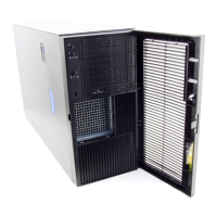
Intel® Server System S7000FC4UR TPS Memory Riser
Revision 1.0
49
The following table lists the FBD maximum bandwidths supported by the memory sub-system.
Table 11. Memory Riser Max Memory Bandwidth
533 Channel BW
Theoretical = 6.4GB/s
Max BW
per Channel
Max BW*
per DIMM
1 DIMMs/Channel 2.8GB/s 2.80GB/s
2 DIMMs/Channel 3.5GB/s 1.75GB/s
4 DIMMs/Channel 3.8GB/s 0.95GB/s
8 DIMMs/Channel 3.8GB/s 0.48GB/s
667 Channel BW
Theoretical = 8.0GB/s
Max BW
per Channel
Max BW*
per DIMM
1 DIMMs/Channel 3.0GB/s 3.0GB/s
2 DIMMs/Channel 3.9GB/s 1.95GB/s
4 DIMMs/Channel 4.6GB/s 1.15GB/s
8 DIMMs/Channel 4.6GB/s 0.58GB/s
*Note: Assumes FBDIMMs of equal capacity
The FBD memory subsystem can be broken into different segments (see following topology).
The first segment, called the FBD southbound Channel, is a high-speed differential, point to
point, frame-based interface from the Intel
®
7300 Chipset MCH to an Advanced Memory Buffer
(AMB) that resides on the DIMM module. The next segment, called the DDR2 Channel,
represents the interface between the AMB and DDR2 DRAM devices. The AMB takes the
frame-based data packets from the FBD southbound channel and translates them into standard
JEDEC-DDR2 based data and commands. In addition, the AMB also repeats the southbound
data packets from the MCH and sends them on to the second DIMM/AMB in the chain via its
own southbound Channel. This southbound data transfer scheme is repeated for all DIMMs in
the chain or channel (eight DIMMs per channel in the case of the memory riser). The other FBD
segment, called the northbound FBD Channel, represents the path for all data coming from the
DIMMs going northbound to the Intel
®
7300 Chipset MCH. Similar to the southbound Channel
(but in the opposite direction), the data on the northbound Channel gets repeated by each
DIMM/AMB in the chain until it eventually arrives at the MCH.
FBD Channels A and B combine to represent Branch 0, and FBD Channels C and D combine to
represent Branch 1. Each branch controller and every DIMM will receive its own FBD reference
clock. The FBD Channel reference clock is exactly half the DDR2 reference clock. The PLL
within the AMB on the DIMM module will multiply the input reference clock input by two and
deliver the appropriate clock speed to all of the DDR2 DRAM devices.
 Loading...