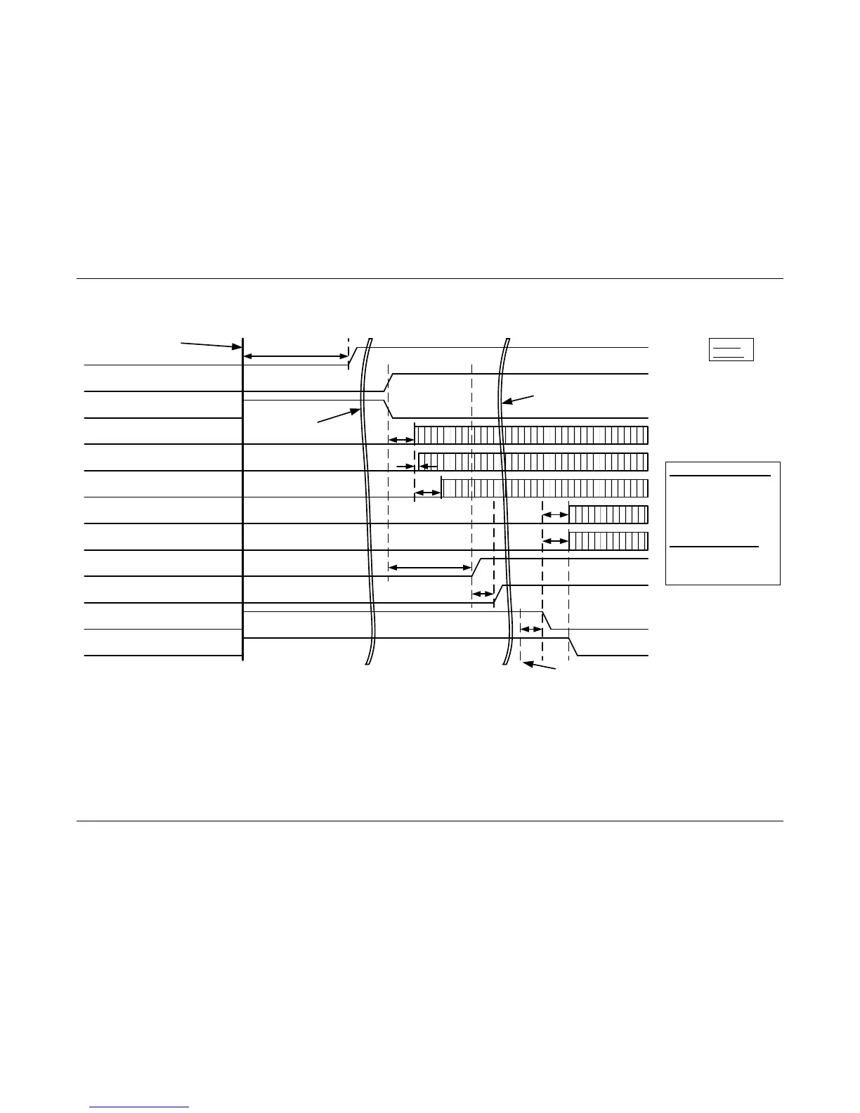
2.2.23.2 Reset Sequencing Diagram
All VRs PowerGood
PLTRST_N/PCIRST_N
CK410B Output Clocks
DB1900G-PCIe Output Clocks
100ms
(min)
DB1200G-Host Output Clocks
Rev 2.0
12/19/06
DB1900G-FBD BR0 Output Clocks
DB1900G-FBD BR1 Output Clocks
SYS_PWRGD Copies:
· SYS_PWRGD_PLD
· SYS_PWRGD
· SYS_PWRGD_BUFF1
· SYS_PWRGD_BUFF2
· SYS_PWRGD_BUFF3
PLTRST_N Copies:
· PLTRST_N
· PLTRST_BUFF1_N
· PLTRST_BUFF2_N
CK410B_PWRGD_N
SYS_PWRGD
RSM_RST_N
Valid Clocks
Valid Clocks
Valid Clocks
Valid Clocks
Valid Clocks
1.8ms
(max)
1ms
(max)
Section below describes this
undefined amount of time
AC Power Applied
240ms
(min)
Time Not to Scale
1.8ms
(max)
4.5ns
(max)
2.25ms
(min)
2.25ms
(min)
FBD_CLKEN_N
FBD_RESET
FBD Gear Ratios Set
1ms
(min)
Power Sequencing Diagram
describes this undefined time
Figure 7. Main Board Reset Sequencing Diagram

 Loading...