www.dadehpardazan.ir 88594014-15
3.3 I/O Signal Allocations
3-27
<Input signal polarities>
Input signal polarities are as follows when sequence input circuit is connected to a sink circuit. If connected to
a source circuit, polarities are reversed. For details, refer to 3.4.2 Sequence Input Circuit.
(4) Checking Input Signals
Input signal status can be checked using the input signal monitor (Un005). As for the input signal monitor
(Un005), refer to 8.6 Monitoring Input Signals.
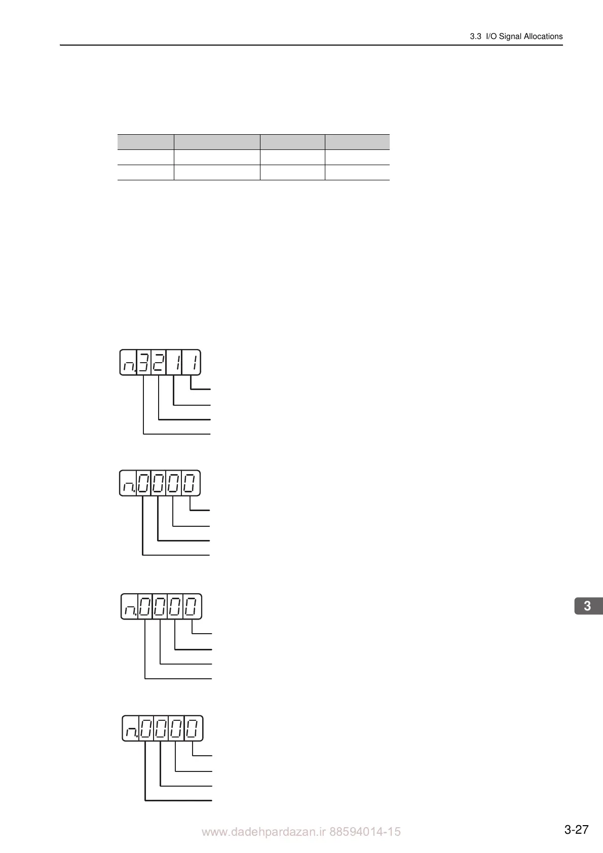
3.3.2 Output Signal Allocations
Output signals can be allocated to I/O signal connectors (CN1) in accordance with the parameter setting of
Pn50E, Pn50F, Pn510, and Pn512.
(1) Checking Factory Settings
Factory settings can be checked using the following parameters.
Signal Level Voltage Level Contact
ON Low (L) level 0 V Close
OFF High (H) level 24 V Open
Pn50E
Allocates /COIN signal to CN1-25, -26.
Allocates /V-CMP signal to CN1-25, -26.
Allocates /TGON signal to CN1-27, -28.
Allocates /S-RDY signal to CN1-29, -30.
Pn50F
Not to use /CLT signal.
Not to use /VLT signal.
Not to use /BK signal.
Not to use /WARN signal.
Pn510
Not to use /NEAR signal.
Reserved (Cannot be changed)
Not to use /PSELA signal.
Reserved (Cannot be changed)
Pn512
Not to invert CN1-25, -26 output signals.
Not to invert CN1-27, -28 output signals.
Not to invert CN1-29, -30 output signals.
Reserved (Cannot be changed)