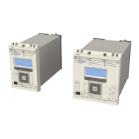
Recommended Scheme Opto Connections and Settings
I/O option G or J I/O Option F I/O Option C
Opto Input 1
(Mode Setting)
Opto Input 2
(Mode Setting)
Opto Input 4
(Mode Setting)
Opto Input 5
(Mode Setting)
Opto Input 6
(Mode Setting)
Opto Input 9
(Mode Setting)
Opto Input 10
(Mode Setting)
Opto Input 11
(Mode Setting)
Opto A
(T
CS)
Opto B
(TCS)
Opto A
(TCS)
Opto B
(TCS)
-
(NORMAL)
Opto A
(TCS)
Opto B
(TCS)
-
(NORMAL)
I/O Option H
5.4.1 RESISTOR VALUES
The TCS opto-inputs sink a constant current of 2 mA.The values of external resistors R1 and R2 are chosen to limit
the curr
ent to a maximum of 60 mA in the event that an opto-input becomes shorted. The values of these resistors
depend on the trip circuit voltage. To achieve compliance with ENA Specification H7, we have carried out extensive
testing and we recommended the following resistors values.
Trip Circuit Voltage Resistor R1 and R2 (ohms)
24/27 620 Ohms at 2 Watts
30/34 820 Ohms at 2 Watts
48/54 1.2 kOhms at 5 Watts
110/125 2.7 kOhms at 10 Watts
220/250 5.2 kOhms at 15 Watts
For the momentary tripping condition, none of the opto-inputs are energised. To tide over this normal CB
operation, a dr
op-off time delay of about 400 ms is added in the PSL.
Warning:
If y
our IED has Opto Mode settings available in the OPTO CONFIG column, these
MUST be set to TCS for any corresponding Opto Inputs(s) used for Trip Circuit
Supervision.
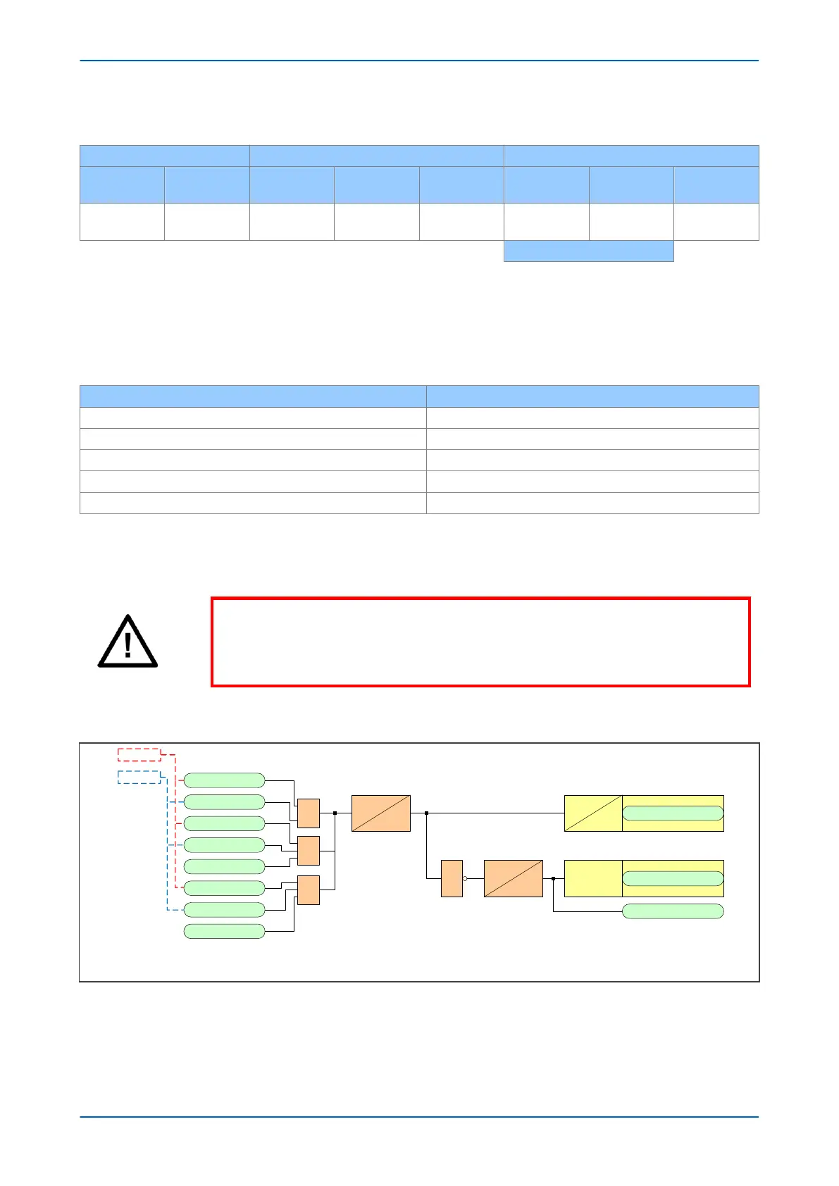
5.4.2 PSL FOR TCS SCHEME 4
Opto input 1
V01223
&
*Output Relay
LED
Use r Alarm
0
400
Dropoff
straig ht
0
0
Latch ing
Opto input 2
1
pickup
0
50
*NC stands for Normally Clo sed.
Opto input 4
Opto input 5
Opto input 6
Opto input 9
Opto input 10
Opto input 11
1
1
Opto A
Opto B
Figure 142: PSL for TCS Scheme 4
P24xM Chapter 14 - Supervision
P24xM-TM-EN-2.1 287
 Loading...