MAX32660 User Guide
Maxim Integrated Page 164 of 195
Equation 13-3: SCK Low Time
13.3.7 Clock Phase and Polarity Control
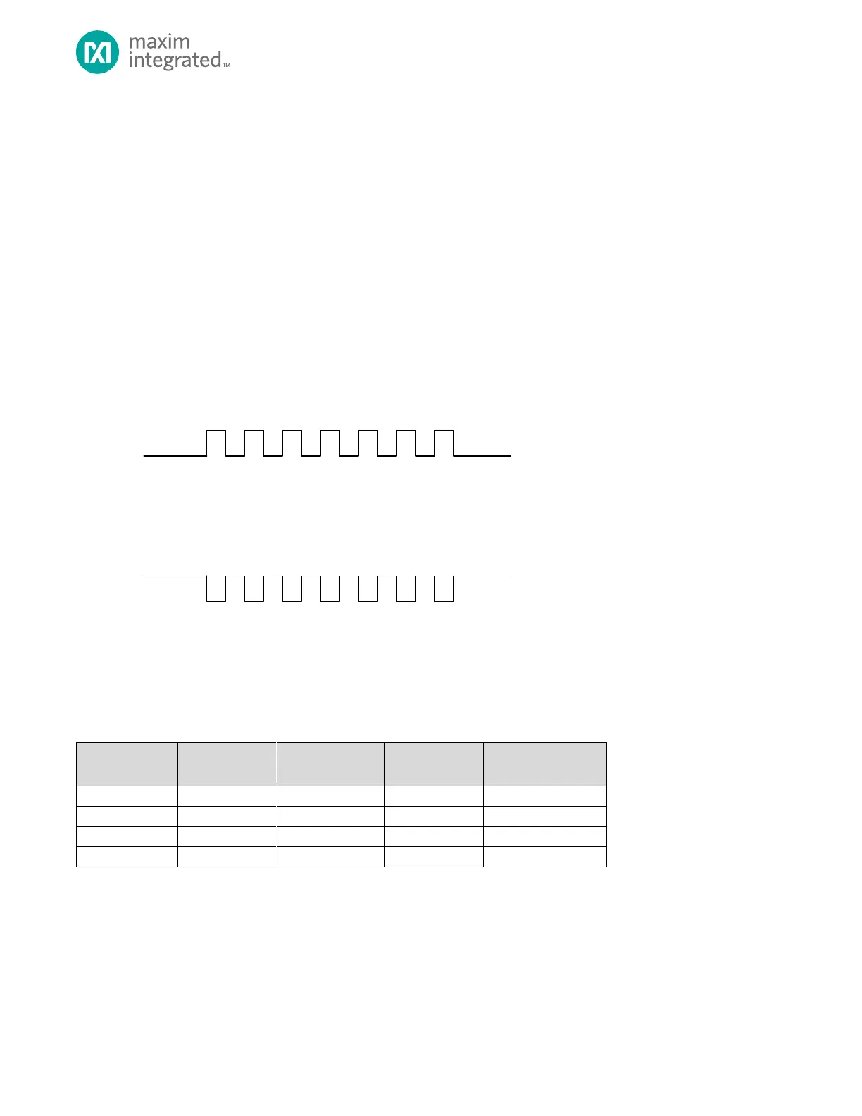
SPIn supports four combinations of clock and phase polarity as shown in Table 13-4, below. Clock polarity is controlled using
the bit SPI0_CTRL2.clk_pol and determines if the clock is active high or active low as shown in Figure 13-5. Clock polarity
does not affect the transfer format for SPI. Clock phase determines when the data must be stable for sampling. Setting the
clock phase to 0, SPI0_CTRL2.clk_pha = 0, dictates the SPI data is sampled on the initial SPI clock edge regardless of clock
polarity. Phase 1, SPI0_CTRL2.clk_pha = 1, results in data sample occurring on the second edge of the clock regardless of
clock polarity.
Figure 13-5: SPI Clock Polarity
For proper data transmission, the clock phase and polarity must be identical for the SPI master and slave. The master
always places data on the MOSI line a half-cycle before the SCLK edge for the slave to latch the data.
Table 13-4. Clock Phase and Polarity Operation
13.3.8 Transfer Format Phase 0
Figure 13-7 is the timing diagram for an SPI 16-bit transfer in which the clock phase is cleared (SPI0_CTRL2.clk_pha = 0). The
two SCK waveforms show active low (SPI0_CTRL2.clk_pol = 0) and active high (SPI0_CTRL2.clk_pol = 1). The diagram may be
interpreted as either a master or slave timing diagram since the SCLK, MISO and MOSI pins are directly connected between
the master and the slave.

 Loading...