MAX32660 User Guide
Maxim Integrated Page 19 of 195
3.3.5 Core AHB Interface
3.3.5.1 I-Code
This AHB master is used by the Arm core for instruction fetching from memory instances located in code space from byte
addresses 0x0000 0000 to 0x1FFF FFFF. This bus master is used to fetch instructions from the internal flash memory.
Instructions fetched by this bus master are returned by the instruction cache, which in turn triggers a cache line fill cycle to
fetch instructions from the internal flash memory when a cache miss occurs.
3.3.5.2 D-Code
This AHB master is used by the Arm Cortex-M4 with FPU core for data fetches from memory instances located in code space
from byte addresses 0x0000 0000 to 0x1FFF FFFF. The D-Code AHB master has access to the full internal flash memory.
3.3.5.3 System
This AHB master is used by the Arm core for all instruction fetches and data read and write operations involving the SRAM.
The APB mapped peripherals (through the AHB-to-APB bridge) and AHB mapped peripheral and memory areas are also
accessed using this bus master.
3.3.6 AHB Master
3.3.6.1 Standard DMA
The Standard DMA bus master has access to all off-core memory areas accessible by the System bus. It does not have
access to the Arm Private Peripheral Bus area.
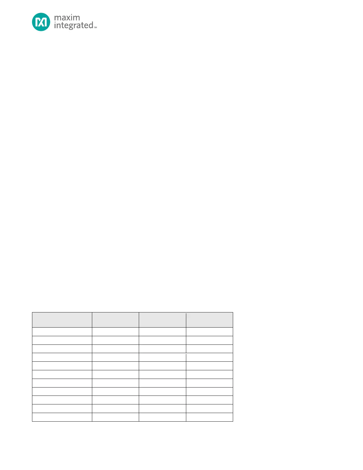
3.4 Peripheral Register Map
Table 3-1, below, contains the base address for each of the APB mapped peripherals. The base address for a given
peripheral is the start of the register map for the peripheral. For a given peripheral, the address for a register within the
peripheral is defined as the peripheral base address
Table 3-1: APB Peripheral Base Address Map