MAX32660 User Guide
Maxim Integrated Page 173 of 195
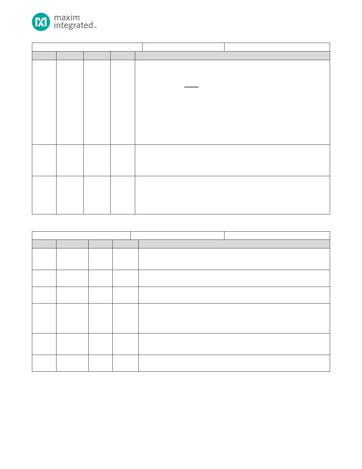
SPI Master Clock Configuration Register
System Clock to SPI Clock Scale Factor
Scales the Peripheral Clock (PCLK) by 2
scale
to generate the SPI module clock.
0x0 - 0x8: Scales the system clock by the set value to generate the internal SPI clock
0x9 - 0xF: Invalid
Note: The microcontroller System Clock is scaled by scale to generate the internal SPI
clock. The external SPI clock, SCLK, is generated by setting the low cycle time, low, and
the high cycle time, hi.
Note: If scale=0, hi=0, and lo=0, character sizes of 2 and 10 bits are not supported.
SCLK Hi Clock Cycles Control
0x0: Hi duty cycle control disabled. Only valid if scale = 0.
0x1 0xF: Number of internal SPI clocks that SCLK is high.
Note: If scale=0, hi=0, and lo=0, character sizes of 2 and 10 bits are not supported.
SCLK Low Clock Cycles Control
0x0: Low duty cycle control disabled. Only valid if SPI0_CLK_CFG.scale = 0.
0x1 0xF: Number of internal SPI clocks that SCLK is low
Note: If SPI0_CLK_CFG.scale=0, SPI0_CLK_CFG.hi=0, and SPI0_CLK_CFG.low=0, character
sizes of 2 and 10 bits are not supported.
Table 13-12: SPI DMA Control Registers
RX DMA Enable
0: RX DMA is disabled. Any pending DMA requests are cleared
1: RX DMA is enabled
Reserved for Future Use
Do not modify this field.
Number of Bytes in the RX FIFO
Read returns the number of bytes currently in the RX FIFO
Clear the RX FIFO
1: Clear the RX FIFO and any pending RX FIFO flags in SPI0_INT_FL. This should be
done when the RX FIFO is inactive.
Writing a 0 has no effect.
RX FIFO Enabled
0: RX FIFO disabled
1: RX FIFO enabled
Reserved for Future Use
Do not modify this field.