MAX32660 User Guide
Maxim Integrated Page 167 of 195
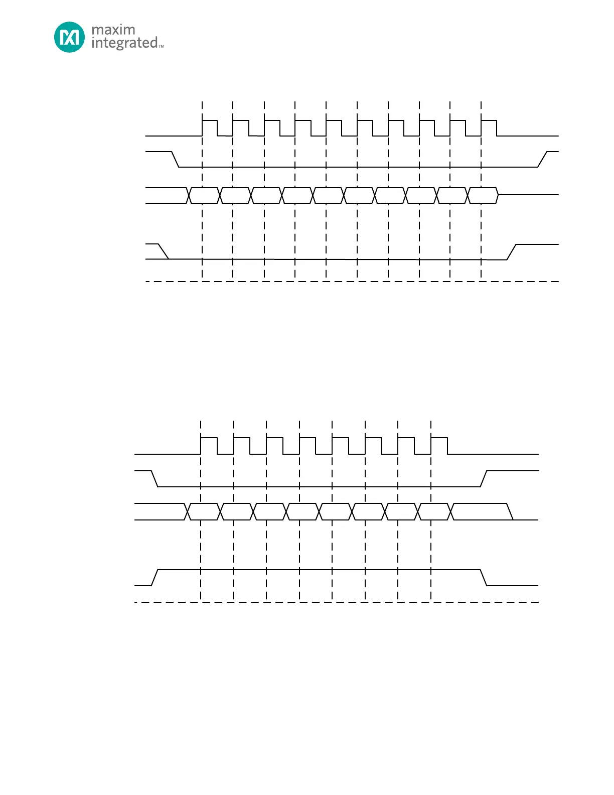
Figure 13-8: Three-Wire SPI Read
13.3.10.2 Write Transaction
Figure 13-9 shows a three-wire SPI write transaction. The direction is set to write by disabling the receive FIFO
(SPI0_DMA.rx_fifo_en = 0) and enabling the transmit FIFO (SPI0_DMA.tx_fifo_en = 1). The SPI0_MOSI(SISO) pin is
automatically set as to an output by hardware based on the FIFO enable bits. Data should be loaded to the transmit FIFO for
the write.
Figure 13-9: Three-Wire SPI Write
13.3.11 Additional Configuration
Interrupt events are configured using the SPI0_INT_EN register.
Wakeup events are configured using the SPI0_WAKE_EN register.