MAX32660 User Guide
Maxim Integrated Page 59 of 195
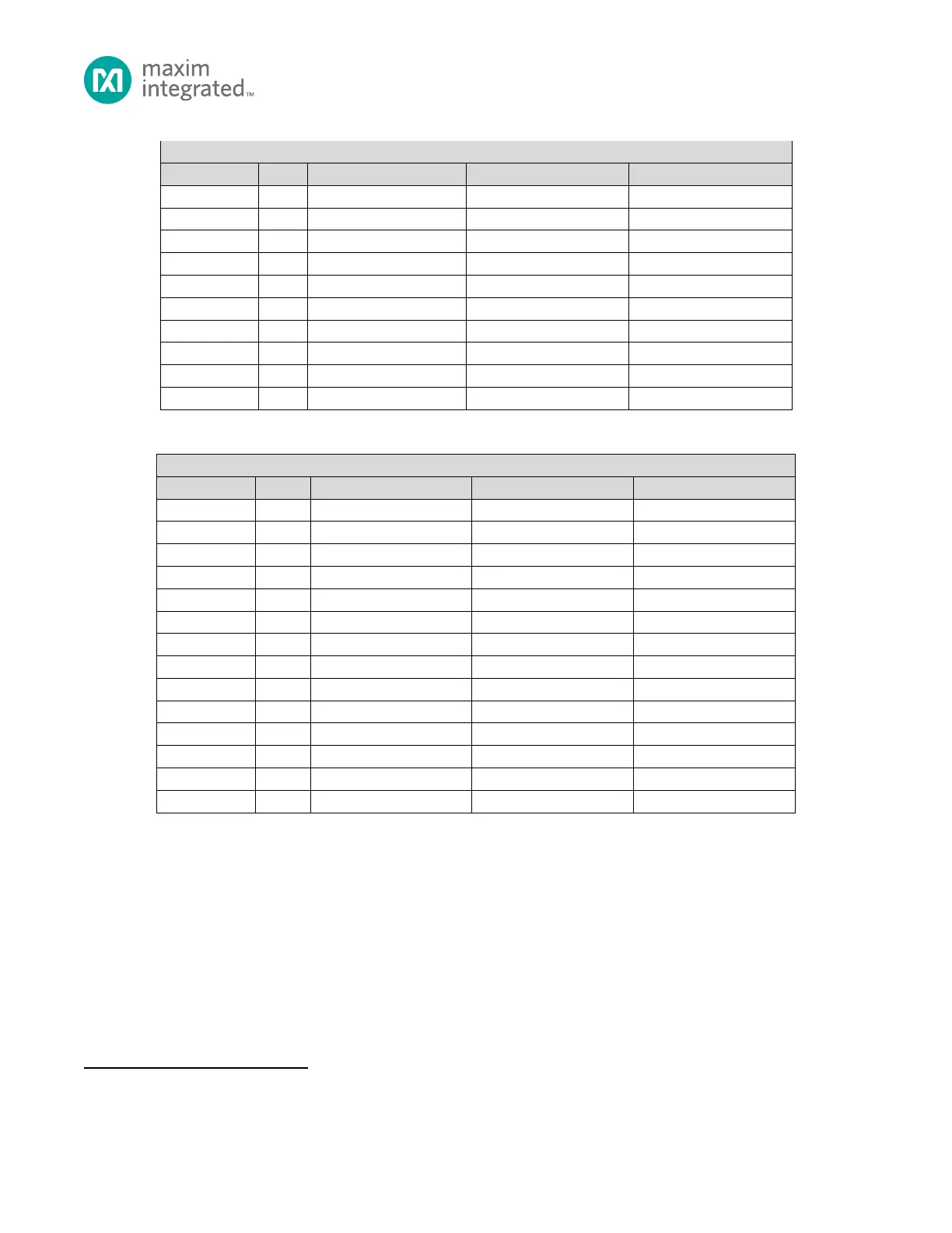
Table 6-1: GPIO Port, Pin Name and Alternate Function Matrix, 16-WLP
Table 6-2: GPIO Port, Pin Name and Alternate Function Matrix, 20-TQFN
6.2 Power-On-Reset Configuration
During a power-on-reset event all I/O default to GPIO mode as inputs floating except the SWD JTAG pins P0.0 and P0.1. The
SWD JTAG pins always default to Alternate Function 1 enabled and the SWD JTAG is enabled.
This alternate function signal is mappable to more than one GPIO pin but there is only one instance of this peripheral in the MAX32660.
I2S_BCLK, I2S_LRCLK, I2S_SDK, I2S_SDO when the I2S function is enabled.
GPIO with I2C as an Alternate Function do not support slew rate control and only support two output drive strength modes.