MAX32660 User Guide
Maxim Integrated Page 172 of 195
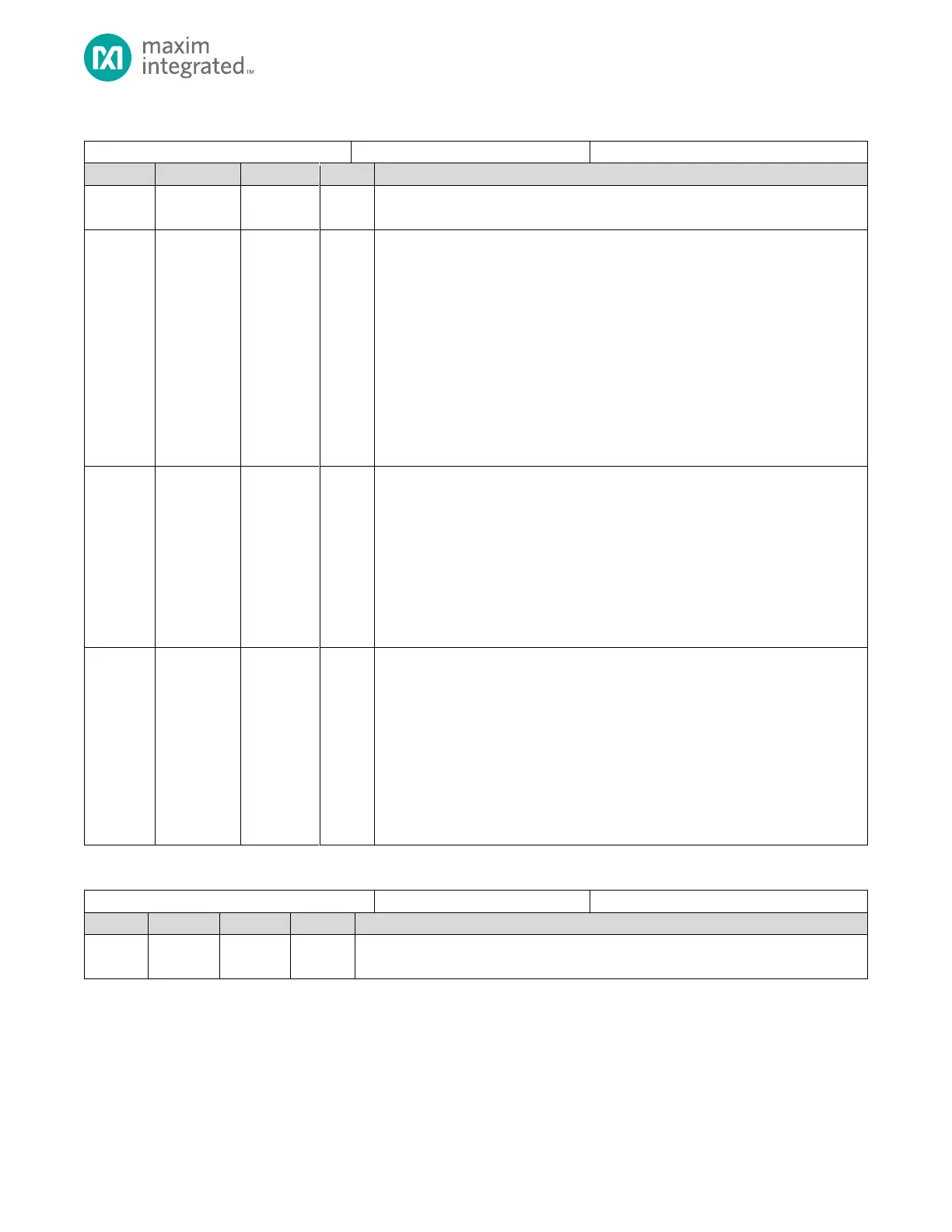
Table 13-10: SPI Slave Select Timing Register
Reserved for Future Use
Do not modify this field.
SS Inactive Clock Delay
This is the time SS is inactive, and the bus is inactive between character
transmission.
It is the number of system clock cycles from the time a character is transmitted, and
SS is inactive to the time SS is active and a new character is transmitted.
0: 256
1: 1
2: 2
3:3
254: 254
255: 255
Slave Select Active After Last SCLK
Number of system clock cycles that SS is active from the last SCLK edge to when SS is
inactive. 0: 256
1: 1
2: 2
3:3
254: 254
255: 255
Slave Select Active to First SCLK
Number of system clock cycles between the time SS is asserted until the first SCLK
edge.
0: 256
1: 1
2: 2
3:3
254: 254
255: 255
Table 13-11: SPI Master Clock Configuration Registers
SPI Master Clock Configuration Register
Reserved for Future Use
Do not modify this field.