MAX32660 User Guide
Maxim Integrated Page 87 of 195
8.6 Flushing the UART FIFOs
The FIFOs can be flushed independently by setting UARTn_CTRL0.rxflush to 1 for the RX FIFO and UARTn_CTRL0.txflush. to 1
for the TX FIFO. The TX FIFO and RX FIFO are automatically flushed if the UART is disabled by clearing the
UARTn_CTRL0.enable field (UARTn_CTRL0.enable = 0).
8.7 Hardware Flow Control
When hardware flow control is enabled, the CTS (Clear-to-send) and RTS (Request-to-Send) external signals are directly
managed by hardware without CPU intervention. RTS and CTS are active when flow control is enabled by setting the
register bit UARTn_CTRL0.flowctl=1. The polarity of the CTS/RTS signals are configured with register bit
UARTn_CTRL0.flowpol and can be active low or active high.
In operation, the host UART that wants to transmit data asserts the RTS output pin and waits for the CTS input pin to be
asserted. If CTS is asserted, then the host UART begins transmitting data to the slave UART. If during the transmission the
host UART notices CTS is deasserted, the host UART finishes transmitting the current character and then pauses to wait for
CTS to return to an asserted level before transmitting more data.
If this UART is receiving data, and the RX FIFO reaches the level set in the 6-bit register field UARTn_CTRL1.rts_fifo_lvl, then
the RTS signal of this UART is deasserted, informing the transmitting UART to stop sending data to this UART to prevent
data overflow. Transmission resumes when the level of the RX FIFO drops below UARTn_CTRL1.rts_fifo_lvl, which
automatically asserts RTS.
8.8 UART Registers
The UART0 base peripheral address is 0x4004 2000 and the UART1 base peripheral address is 0x4004 3000. Refer to Table
3-1: APB Peripheral Base Address Map for the addresses of all APB mapped peripherals.
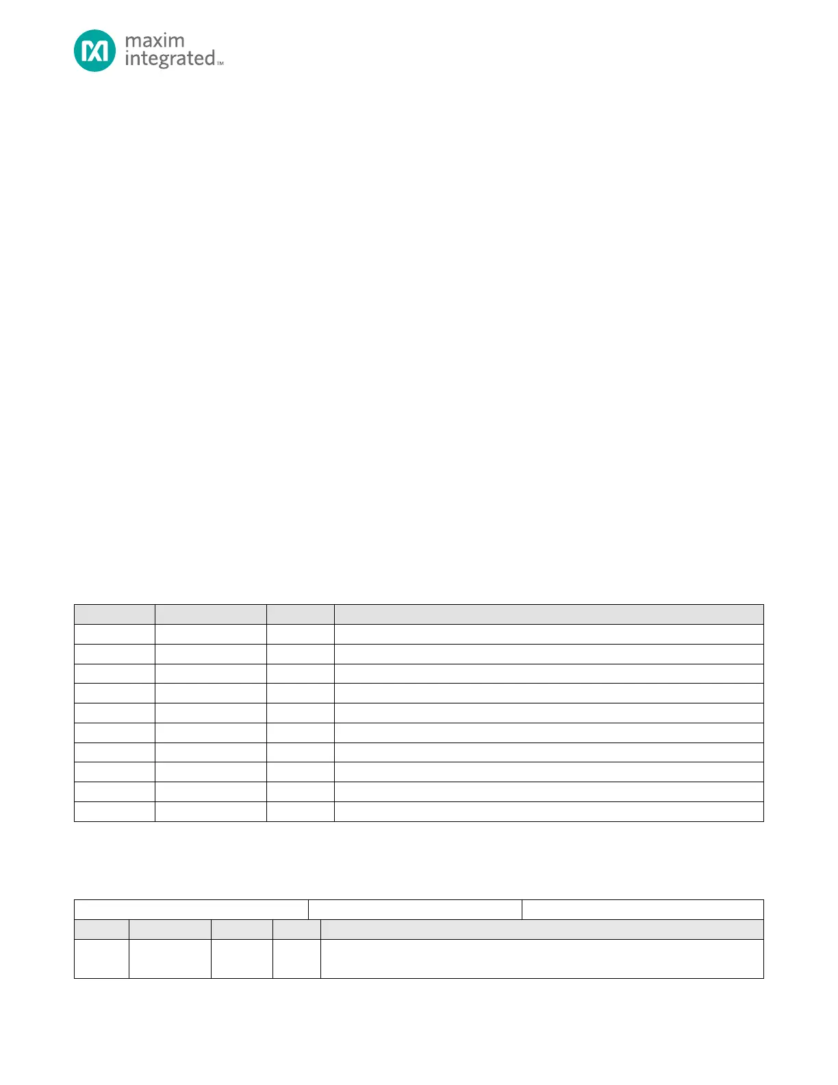
Table 8-2: UART Registers, Offset Addresses and Descriptions