MAX32660 User Guide
Maxim Integrated Page 169 of 195
SPI0 has four Wakeup (WAKE) sources that can wake the core from SLEEP mode when the WAKE event occurs. The
following WAKE events are supported:
• Wake on RX FIFO Full
• Wake on TX FIFO Empty
• Wake on RX FIFO Level crossed
• Wake on TX FIFO Level crossed
13.4 SPI0 Registers
The SPI0 base peripheral address is 0x4004 6000. Refer to Table 3-1: APB Peripheral Base Address Map for the addresses of
all APB mapped peripherals.
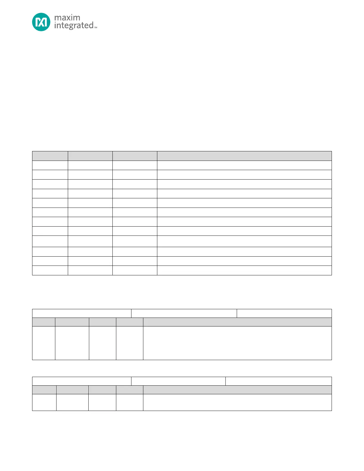
Table 13-5: SPI0 Master Register Addresses and Descriptions
SPI Master Signals Control Register
SPI Transmit Packet Size Register
SPI Static Configuration Register
SPI Slave Select Timing Register
SPI Master Clock Configuration Register
SPI Interrupt Status Flags Register
SPI Interrupt Enable Register
SPI Wakeup Status Flags Register
SPI Wakeup Enable Register
SPI Active Status Register
13.4.1 SPI0 Register Details
Table 13-6: SPI FIFO Data Registers
SPI FIFO Data Register
Reading from this register dequeues data from the receive FIFO.
Writes to this register queues data to the transmit FIFO.
Reads and writes with this register are in 1-byte, 2-byte, or 4-byte widths only.
Table 13-7: SPI Master Signals Control Registers
SPI Master Signals Control Register
Reserved for Future Use
Do not modify this field.

 Loading...