EasyManua.ls Logo

Maxim Integrated MAX32660 - Table 7-3: Source and Destination Address Definition; Table 7-4: Data Movement from Source to DMA FIFO

Maxim Integrated MAX32660
195 pages
Print Icon
To Next Page IconTo Next Page
To Previous Page IconTo Previous Page
Loading...
MAX32660 User Guide
Maxim Integrated Page 73 of 195
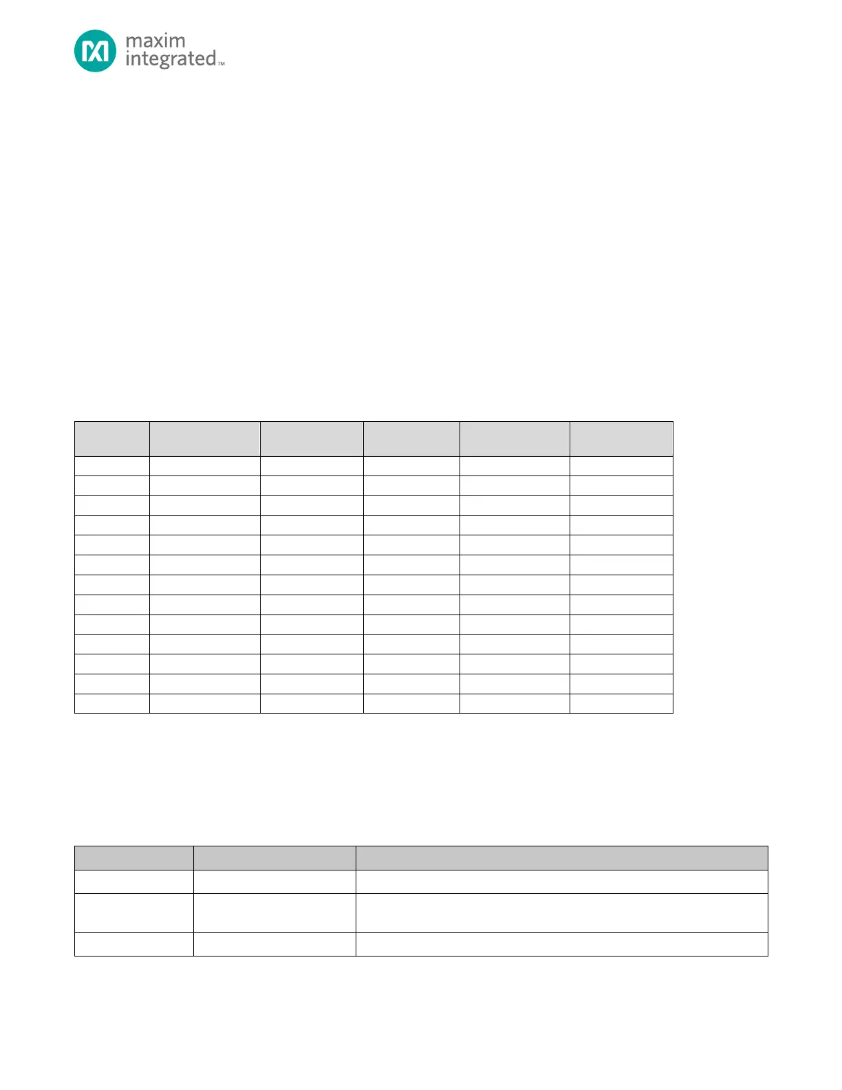
7.3 DMA Source and Destination Addressing
For memory addresses, the DMAn_SRC and DMAn_DST registers are used to program the addresses of the source and
destination. For peripherals, however, the address is fixed based on the DMAn_CFG.reqsel value set.
Table 7-3 shows how the source address, destination address and the address increment controls are constructed based on
the DMAn_CFG.reqsel bitTable 7-3 shows the values for the DMAn_CFG.reqsel bit.

DMAn_CFG.srcinc and the DMAn_CFG.dstinc bits, respectively. If there is a 0 in the column, then the bit is forced to 0. For
peripherals, a value of 0 for the DMAn_CFG.srcinc or DMAn_CFG.dstinc generally indicates the source or destination
DMAn_CFG.reqsel = 0x2, then the transfer is an
SPI1 RX (receive). In this case, the DMAn_CFG.srcinc is fixed to 0 because the source for the SPI1 RX is the SPI1 receive FIFO
address. However, the destination address is programmable, allowing the data from the SPI1 receive FIFO to be written to a
programmable address in memory. The destination starting address is set using the DMAn_DST register and is incremented
automatically if DMAn_CFG.dstinc is set to 1.
Table 7-3: Source and Destination Address Definition
DMAn_CFG
reqsel
Transfer
Source
Address Register
DMAn_CFG
srcinc
Destination
Address Register
DMAn_CFG
dstinc
0x0
Mem-to-Mem
DMAn_SRC
Programmable
DMAn_DST
Programmable
0x1
SPI0 RX
DMAn_SRC
0
DMAn_DST
Programmable
0x2
SPI1 RX
DMAn_SRC
0
DMAn_DST
Programmable
0x4
UART0 RX
DMAn_SRC
0
DMAn_DST
Programmable
0x5
UART1 RX
DMAn_SRC
0
DMAn_DST
Programmable
0x7
I2C0 RX
DMAn_SRC
0
DMAn_DST
Programmable
0x8
I2C1 RX
DMAn_SRC
0
DMAn_DST
Programmable
0x21
SPI0 TX
DMAn_SRC
Programmable
DMAn_DST
0
0x22
SPI1 TX
DMAn_SRC
Programmable
DMAn_DST
0
0x24
UART0 TX
DMAn_SRC
Programmable
DMAn_DST
0
0x25
UART1 TX
DMAn_SRC
Programmable
DMAn_DST
0
0x27
I2C0 TX
DMAn_SRC
Programmable
DMAn_DST
0
0x28
I2C1 TX
DMAn_SRC
Programmable
DMAn_DST
0
7.4 Data Movement from Source to DMA FIFO
Table 7-4 shows the register and bit fields used to control the movement of data into DMA FIFO. The source is a peripheral
or memory.
Table 7-4: Data movement from source to DMA FIFO
Register/Bit Field
Description
Comments
DMAn_SRC
Source address
If the increment enable is set, this increments on every read cycle of the burst.
DMAn_CNT
Number of bytes to transfer
before a CTZ condition occurs
This register is decremented on each read of the burst.
DMAn_CFG.brst
Burst size (1-32)
This determines the maximum number of bytes moved during the burst read.

Table of Contents

Related product manuals