MAX32660 User Guide
Maxim Integrated Page 165 of 195
In the case of multi-character transfers with SS0 remaining asserted between characters, the output data will change at the
end of the Bit0 (final clock edge) to reflect the output value for Bit15 of the next character.
Figure 13-6. SPI Timing (SPI0_CTRL2.clk_pha = 0)
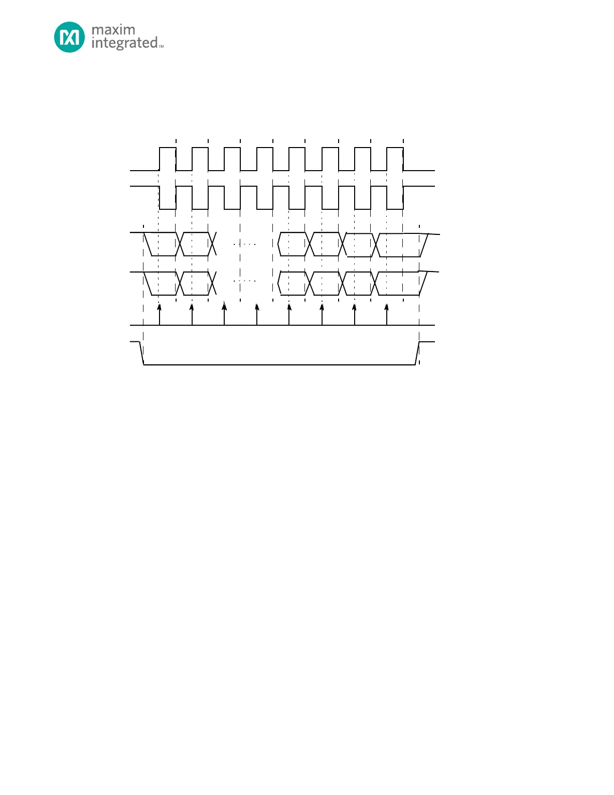
13.3.9 Transfer Format Phase 1
Figure 13-7 is the timing diagram for an SPI transfer in which the clock phase is set (SPI0_CTRL2.clk_pha = 1). The two SCLK
waveforms show active low (SPI0_CTRL2.clk_pol = 0) and active high (SPI0_CTRL2.clk_pol = 1). The diagram may be
interpreted as either a master or slave timing diagram since the SCLK, MISO and MOSI pins are directly connected between
the master and the slave.
In the case of multi-character transfers with SS0 remaining asserted between characters, the bit 0 output data will remain
stable until the clock edge which starts bit 15 of the next character or until the SS0 deasserts at the end of the transfer.