MAX32660 User Guide
Maxim Integrated Page 42 of 195
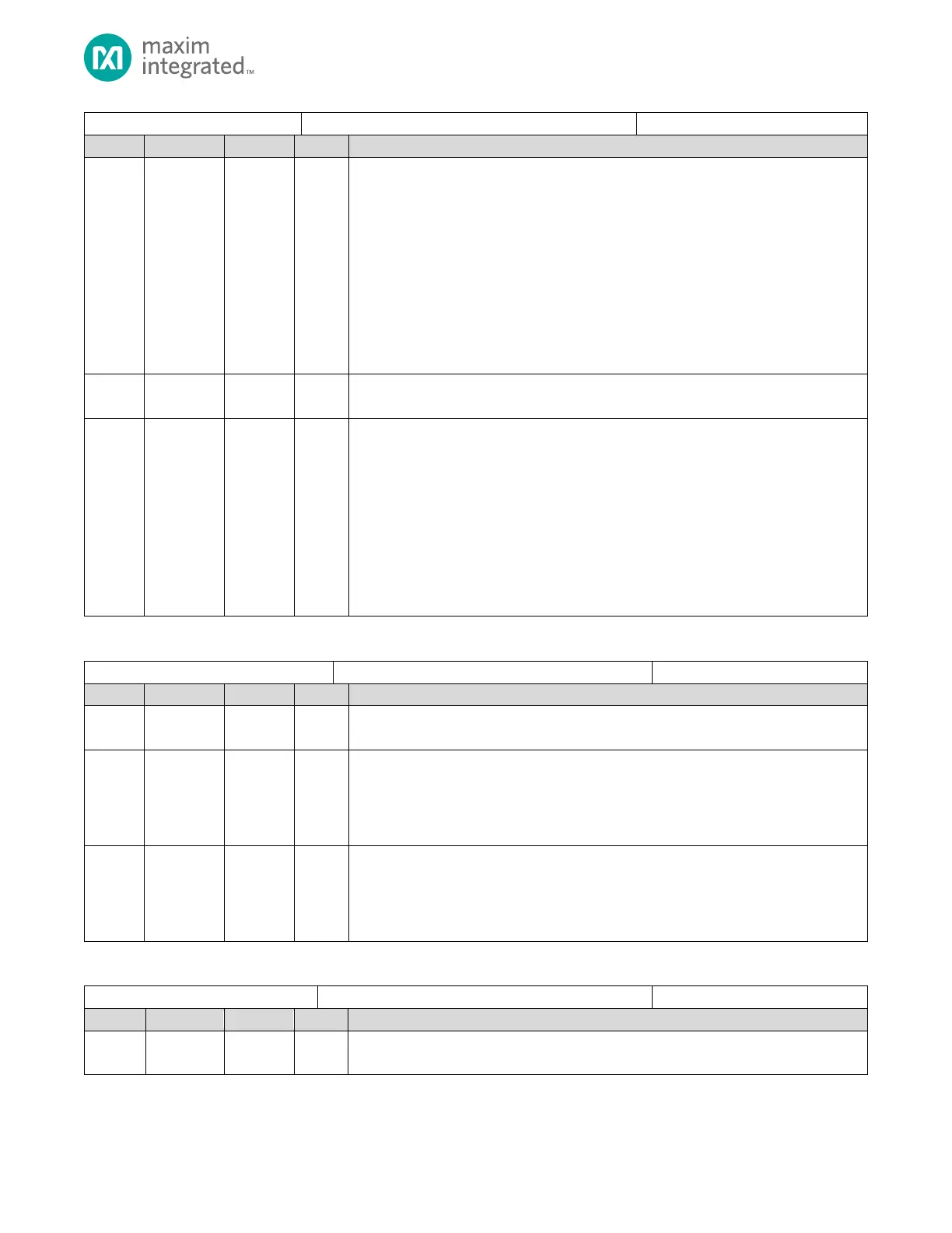
Memory Clock Control Register
System RAM 0 Light Sleep Enable
Set this field to 1 to enable Light Sleep for System RAM 0 (0x2000 0000 - 0x2000 3FFF). If
light sleep is enabled, the System RAM contents are retained but the Data Memory
cannot be read.
0: System RAM 0 is Active.
1: System RAM 0 is in Light Sleep mode.
Note: Any reset event that results in RAM reset will reset the RAM regardless of the state
of this field.
Note: To put RAM in a shutdown mode that removes all power from the RAM and reset
the RAM contents, use the register PWRSEQ_LPMEMSD “Low Power Mode RAM Shut
Down Control”.
Reserved for Future Use
Do not modify this field.
Flash Wait States
Number of wait-states (system clock cycles) for internal flash read access. Refer to
section Flash Wait States for additional information.
0: Reserved for Future Use.
1: 1 Wait State (1 System Clock)
2: 2 Wait States
3: 3 Wait States
4: 4 Wait States (Minimum value for HFIO=System Clock=96MHz)
5: 5 Wait States (Reset default)
6: 6 Wait States
7: 7 Wait States
Table 4-19: Memory Zeroization Control Register
Memory Zeroization Control Register
Reserved for Future Use
Do not modify this field.
Internal Cache Data and Tag RAM Zeroization
RAM. The bit is set to 0 by hardware when the operation is complete.
0: Operation complete
1: Zeroize memory
System Data RAM Zeroization
Write 1 to clear the contents of the Internal Data RAM, all ranges. The bit is set to 0 by
hardware when the operation is complete.
0: Operation complete
1: Zeroize memory
Table 4-20: System Status Flag Register
System Status Flag Register
Reserved for Future Use
Do not modify this field.