EasyManua.ls Logo

Maxim Integrated MAX32660 - Figure 13-7. SPI Timing (Spi0_Ctrl2.Clk_Pha = 1)

Maxim Integrated MAX32660
195 pages
Print Icon
To Next Page IconTo Next Page
To Previous Page IconTo Previous Page
Loading...
MAX32660 User Guide
Maxim Integrated Page 166 of 195
Figure 13-7. SPI Timing (SPI0_CTRL2.clk_pha = 1)
SCLK
(CLKPOL = 0)
SCLK
(CLKPOL = 1)
Bit15
Bit14
Bit3 Bit2 Bit1 Bit0MOSI
Bit15 Bit14 Bit3 Bit2 Bit1 Bit0MISO
Input Sample Time
SSEL
13.3.10 Three-Wire SPI Read and Write
In three-wire SPI, read and write transactions are controlled using the SPI FIFO enable bits. For a read transaction, enable
the Receive FIFO and disable the Transmit FIFO.
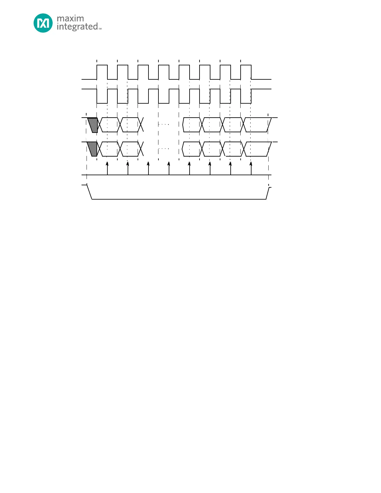
13.3.10.1 Read Transaction
Figure 13-8 shows a three-wire SPI read transaction. The direction is set to a read by enabling the receive FIFO
(SPI0_DMA.rx_fifo_en = 1) and disabling the transmit FIFO (SPI0_DMA.tx_fifo_en = 0). The SPI0_MOSI(SISO) pin is
automatically set as an input by hardware based on the FIFO enable bits.

Table of Contents

Related product manuals