YASKAWA TM.V1000.01 V1000 Drive Installation & Start-Up Manual (Preliminary 01-19-07) 263
5.11 Main Circuit Design
Troubleshooting
5
5.11 Main Circuit Design
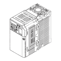
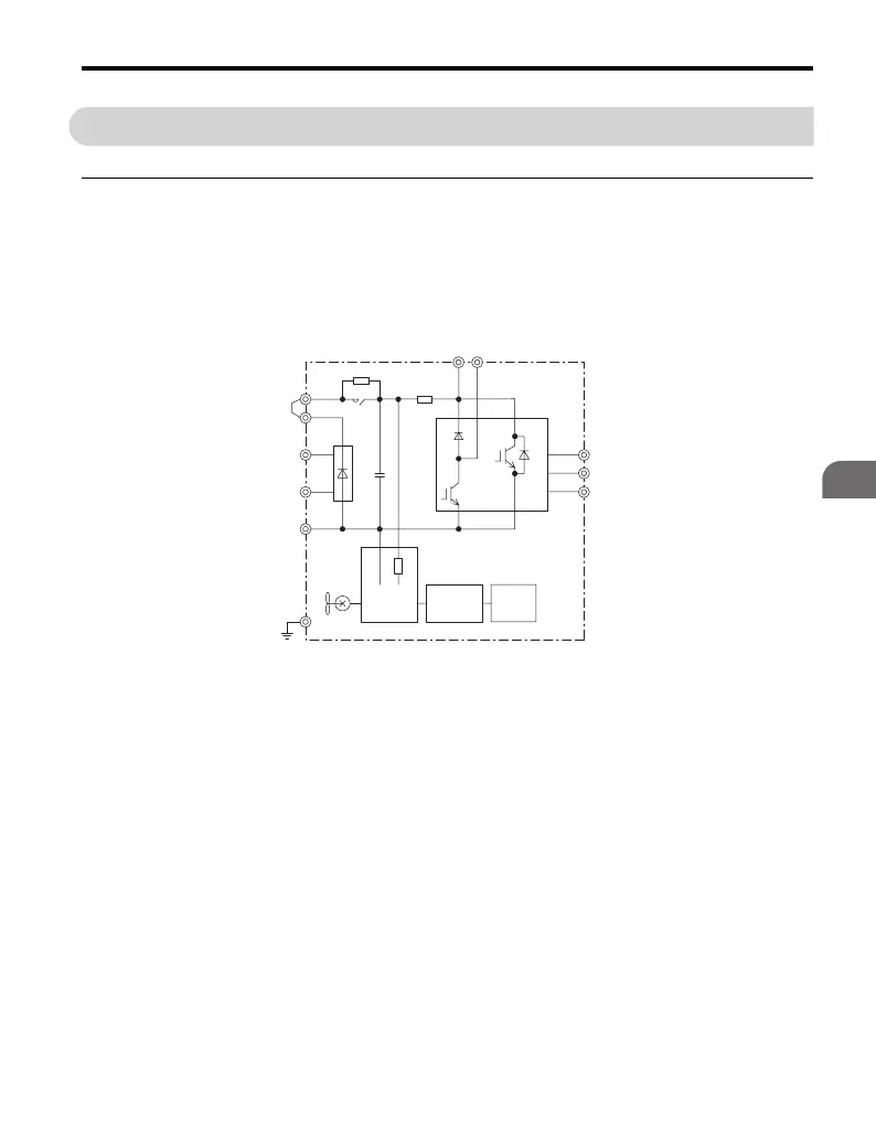
◆ Main Circuit Design (Internal Block Diagram)
Refer to Figure 5.1 and Figure 5.2 for internal block diagrams of the main circuit.
Note: Not all drive models have cooling fans.
■
Single-Phase 200 V Class (CIMR-VBA0001 to CIMR-VBA0012)
Figure 5.1
Figure 5.1 Single-Phase Main Circuit Design
Drive
Shunt
resistor
*Cooling
fan
LED
operator
Control
board
Power
board
R/L1
S/L2
㧗1
㧗2
㧙
+
B1 B2
U/T1
V/T2
W/T3
 Loading...