Memory Interface
ARM DDI 0210C Copyright © 2001, 2004 ARM Limited. All rights reserved. 3-15
Note
The AMBA specification for Advanced High-performance Bus (AHB) and Advanced
System Bus (ASB) requires a pipelined address bus. This means that APE must be
configured HIGH.
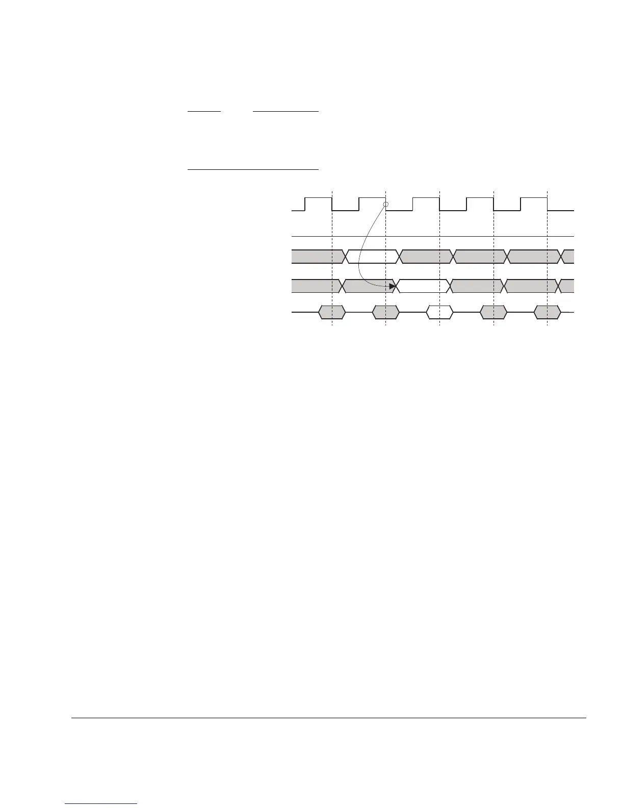
Figure 3-9 Depipelined addresses
Many systems contain a mixture of DRAM, SRAM and ROM. To cater for the different
address timing requirements, APE can be safely changed during the LOW phase of
MCLK. Typically, APE is held at one level during a burst of sequential accesses to one
type of memory. When a nonsequential access occurs, the timing of most systems
enforce a wait state to allow for address decoding. As a result of the address decode,
APE can be driven to the correct value for the particular bank of memory being
accessed. The value of APE can be held until the memory control signals denote
another nonsequential access.
Previous ARM processors included the ALE signal, and this is retained for backwards
compatibility. This signal also enables you to modify the address timing to achieve the
same results as APE, but in a dynamic manner. To obtain clean MCLK low timing of
the address bus by this mechanism, ALE must be driven HIGH with the falling edge of
MCLK, and LOW with the rising edge of MCLK. ALE can simply be the inverse of
MCLK but the delay from MCLK to ALE must be carefully controlled so that the T
ald
timing constraint is achieved. Figure 3-10 on page 3-16 shows how you can use ALE
to achieve SRAM compatible address timing. See Chapter 7 AC and DC Parameters for
details of the exact timing constraints.
MCLK
nMREQ
SEQ
APE
A[31:0]
D[31:0]