AC and DC Parameters
7-18 Copyright © 2001, 2004 ARM Limited. All rights reserved. ARM DDI 0210C
Note
Figure 7-20 on page 7-17 shows the T
bse
, output enable time, parameter and T
bsz
, output
disable time, when the HIGHZ TAP instruction is loaded into the instruction register.
The timing parameters used in Figure 7-20 on page 7-17 are listed in Table 7-20.
Figure 7-21 Output enable and disable times due to data scanning
Note
Figure 7-21 shows the T
bse
, output enable time, parameter and T
bsz
, output disable time
when data scanning, due to different logic levels being scanned through the scan cells
for ABE and DBE.
The timing parameters used in Figure 7-21 are listed in Table 7-20.
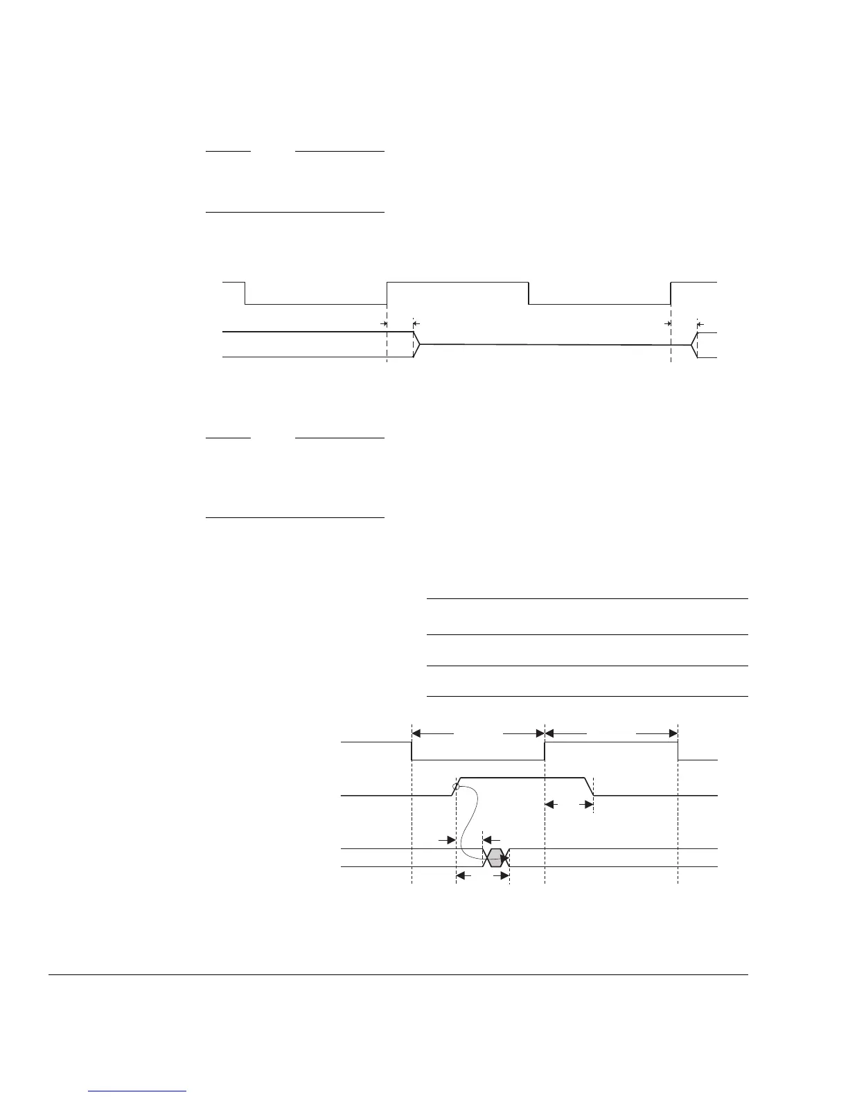
Figure 7-22 ALE address control
T
bsz
T
bse
TCK
A[ ]
D[ ]
Table 7-20 Output enable and disable timing parameters
Symbol Parameter Parameter type
T
bse
Output enable time Maximum
T
bsz
Output disable time Maximum
Phase 2
T
ale
T
ald
MCLK
ALE
A[31:0]
nRW
LOCK
nOPC
nTRANS
MAS[1:0]
Phase 1
T
aleh