Memory Interface
3-30 Copyright © 2001, 2004 ARM Limited. All rights reserved. ARM DDI 0210C
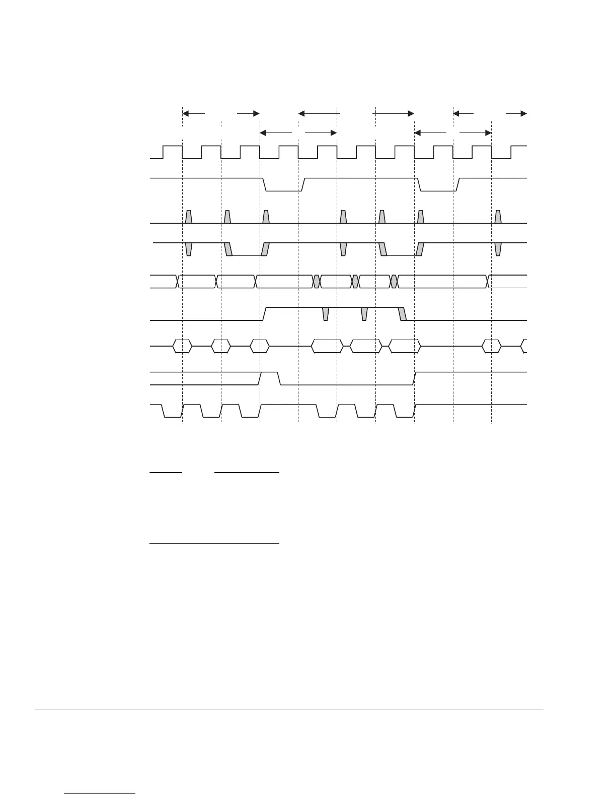
Figure 3-21 Typical system timing
Note
When designing a memory controller, you are strongly advised to sample the values of
nMREQ, SEQ, and the address class signals only when nWAIT is HIGH. This ensures
that the state of the memory controller is not accidentally updated during an extended
bus cycle.
A A+4 A+8 B B+4 B+8 C C+4
MCLK
nMREQ
SEQ
A[31:0]
nRW
nWAIT
D[31:0]
nRAS
nCAS
S S
Cycles Decode Cycles
S S S
Decode
NN
Cycles