EasyManuals Logo

ARM ARM7TDMI User Manual

Default Icon
286 pages
To Next Page IconTo Next Page
To Previous Page IconTo Previous Page
Page #93 background imageLoading...
Page #93 background image
Memory Interface
ARM DDI 0210C Copyright © 2001, 2004 ARM Limited. All rights reserved. 3-23
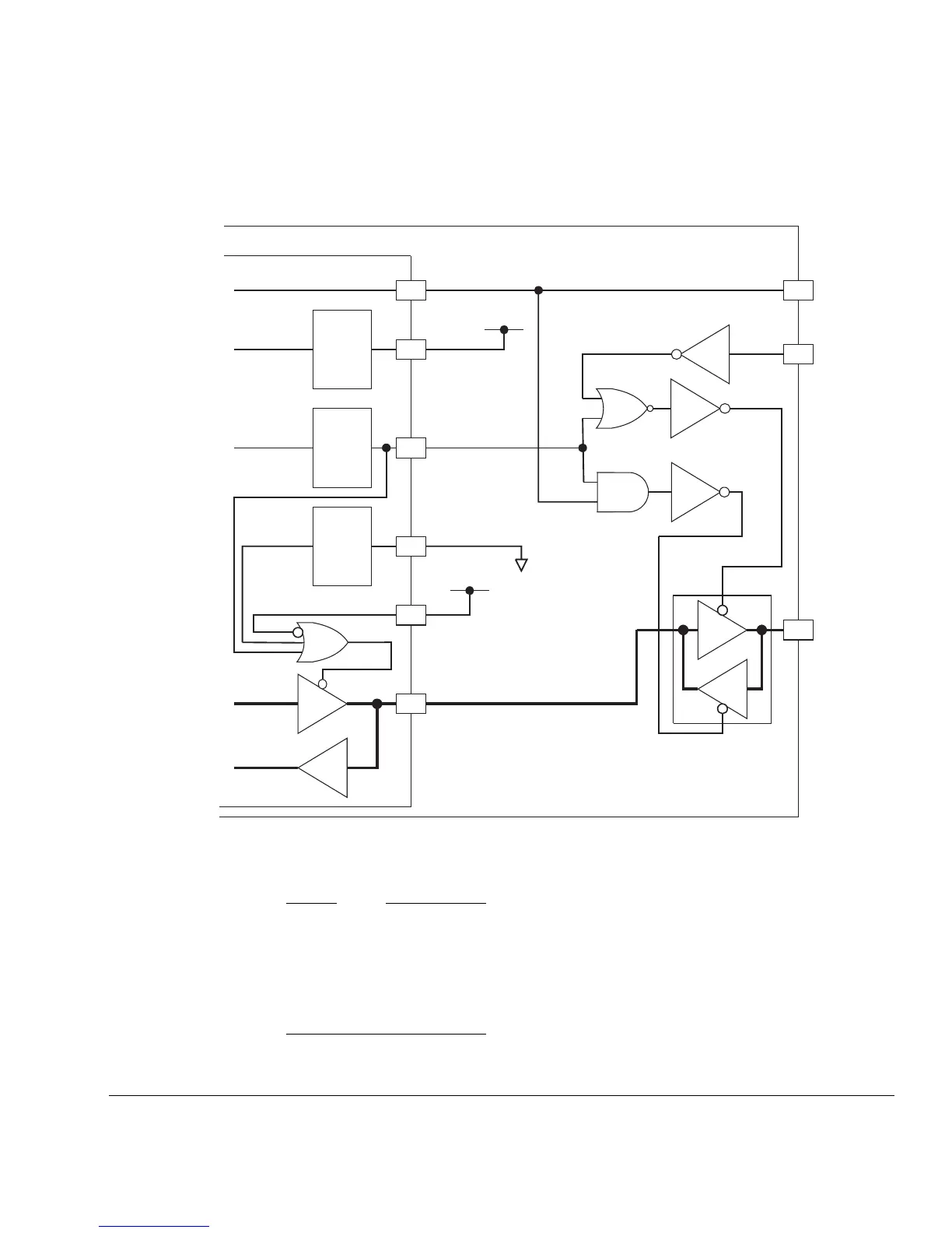
Figure 3-17 Test chip data bus circuit
Note
At the core level, TBE and DBE are inactive, tied HIGH, because in a packaged part
you do not have to manually force the internal buses into a high impedance state. At the
pad level, the test chip signal EDBE is used by the bus control logic to enable the
external memory controller to arbitrate the bus and asynchronously disable the
ARM7TDMI core test chip if necessary.
Scan
cell
Scan
cell
Scan
cell
Vdd
VssVdd
MCLK
DBE
nENOUT
nEDBE
MCLK
EDBE
nENIN
TBE
D[31:0]
XD[31:0]
Pad
ARM7TDMI core
ARM7TDMI test chip or product
nEN1
nEN2

Table of Contents

Other manuals for ARM ARM7TDMI

Questions and Answers:

Question and Answer IconNeed help?

Do you have a question about the ARM ARM7TDMI and is the answer not in the manual?

ARM ARM7TDMI Specifications

General IconGeneral
Data Width32-bit
Cores1
MIPS per MHz0.9
On-chip DebugYes
Instruction SetARM
Pipeline Stages3
Operating VoltageImplementation dependent
Manufacturing ProcessImplementation dependent

Related product manuals