10
10-74
MULTIJUNCTION TIMERS
10.3 TOP (Output-Related 16-Bit Timer)
32180 Group User’s Manual (Rev.1.0)
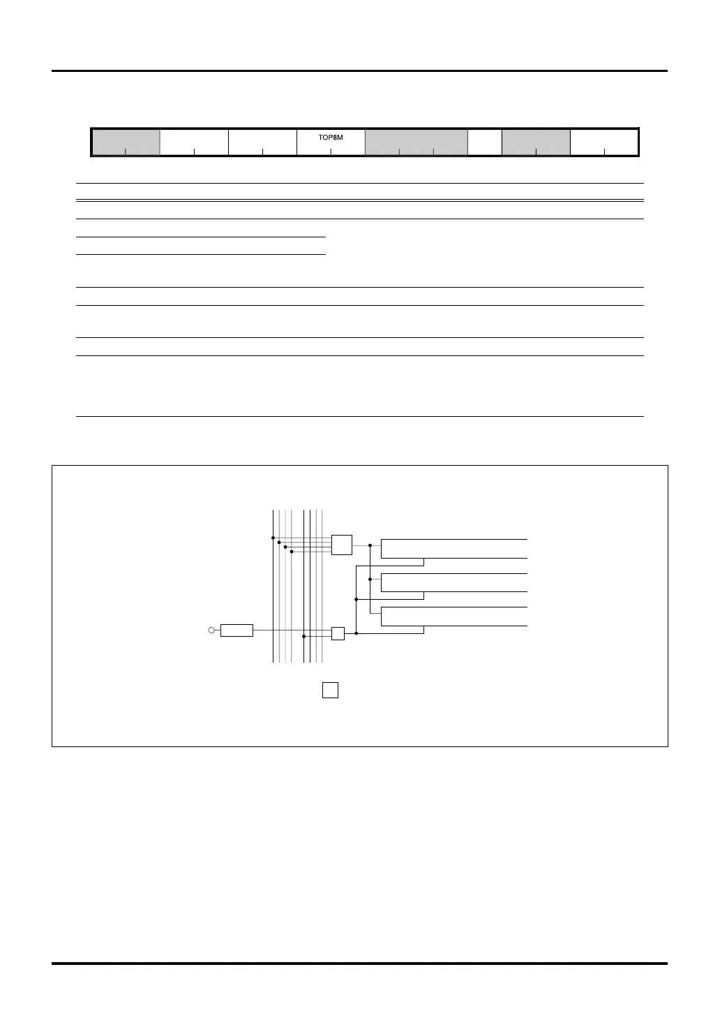
Clock bus Input event bus
3 2 1 0
TIN2 (P152)
TIN2S
S
S
clk
en
TOP 8
clk
en
TOP 9
clk
en
TOP 10
S
: Selector
3 2 1 0
Note: • This diagram only illustrates TOP control registers and is partly omitted.
Figure 10.3.5 Outline Diagram of TOP8–10 Clock and Enable Inputs
TOP8–10 Control Register (TOP810CR) <Address: H’0080 02EA>
b01234567891011121314b15
TOP10M TOP9M TOP8M
T
P
1
ENS
TOP810CKS
00000
00
<After reset: H’0000>
b Bit Name Function R W
0, 1 No function assigned. Fix to "0". 00
2, 3 TOP10M (TOP10 operation mode select bit) 00: Single-shot output mode R W
4, 5 TOP9M (TOP9 operation mode select bit) 01: Delayed single-shot output mode
6, 7 TOP8M (TOP8 operation mode select bit) 10: Continuous output mode
11: – ditto –
8–10 No function assigned. Fix to "0". 00
11 TOP810ENS 0: External TIN2 input R W
TOP8–10 enable source select bit 1: Input event bus 3
12, 13 No function assigned. Fix to "0". 00
14, 15 TOP810CKS 00: Clock bus 0 R W
TOP8–10 clock source select bit 01: Clock bus 1
10: Clock bus 2
11: Clock bus 3
Notes: • This register must always be accessed in halfwords.
• Operation mode can only be set or changed while the counter is inactive.

 Loading...


