17
17-6
RAM BACKUP MODE
32180 Group User's Manual (Rev.1.0)
17.3 Example of RAM Backup for Saving Power Consumption
17.3.2 RAM Backup State
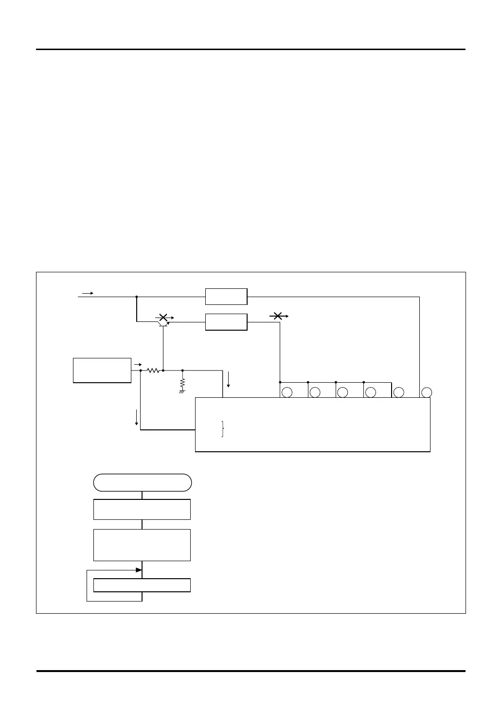
Figure 17.3.3 shows the RAM backup state of the M32R/ECU. Figure 17.3.4 shows a RAM backup sequence.
When the external circuit outputs a low, input on the SBI# or ADnINi pin is pulled low. A low on these input pins
generates a RAM backup signal (A and (a) in Figure 17.3.3). To enable RAM backup mode, make the following
settings:
(1) Create data for RAM check to verify after returning from RAM backup mode to normal mode whether
the RAM data has been retained normally ((b) in Figure 17.3.3).
(2) To materialize low-power operation, set all programmable input/output pins except port X for input
mode (or for output mode, with the output level fixed low) ((c) in Figure 17.3.3).
(3) Set port X for input mode (B and (d) in Figure 17.3.3). This causes the transistor’s base voltage, IB,
to go low, so that the power to all power supply pins except VDDE is shut off (C and D in Figure 17.3.3).
Due to settings in (1) to (3), the VDDE pin voltage goes to 3.0–5.5 V and all other pin voltages drop to 0 V, and
the M32R/ECU is thereby placed in RAM backup mode ((d) in Figure 17.3.3).
Figure 17.3.3 RAM Backup State for Low Power Operation
"L"
B
C
Example of RAM backup processing
(a)
(b)
(c)
(d)
"L"
"L"
"L"
"L"
RAM backup signal
External circuit
Port X
(Note 1)
IB
SBI#
ADnINi
M32R/ECU
(Note 3)
RAM power supply
Regulator
DC IN
Input Output
Regulator
(Note 2)
Output
Note 1: This circuit outputs a low during RAM backup.
Note 2: This port outputs a high when the power is on, and is set for input mode
when in RAM backup mode (one of the port pins selected).
Note 3: These pins are used to detect a RAM backup signal.
Note 4: Determined by the input level on SBI# pin or ADnINi pin.
Note 5: Base voltage IB = 0 causes the power to all power supply pins except VDDE
to stop. See A to D in the above explanation.
0V 0V 0V0V0V
5V
A
Generate a RAM backup signal
(Note 4)
Create data for
backup RAM check
Set the pin connecting to the
transistor's base (port X)
for input mode
(Note 5)
RAM backup mode
D
VREFn VDDEAVCCnVCCE
OSC-VCC
VCC-BUS

 Loading...


